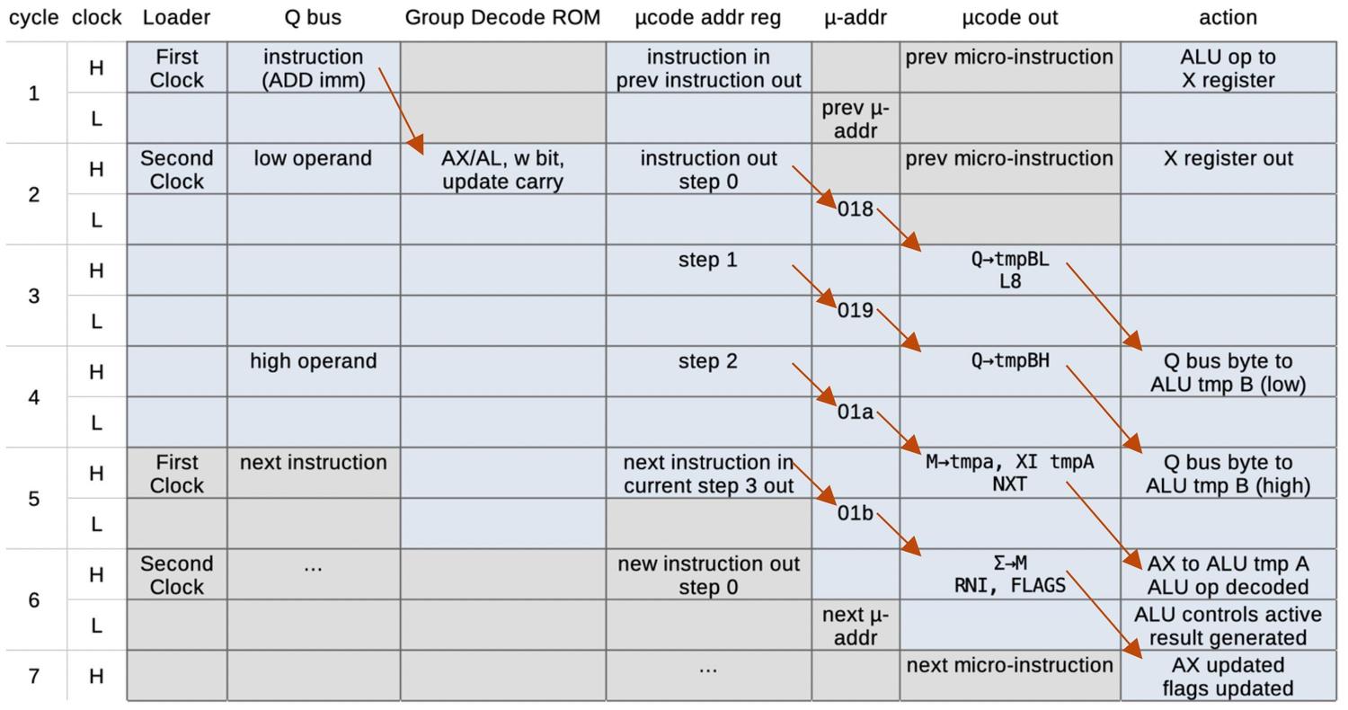
Subject: Undocumented 8086 instructions, explained by the microcode
What happens if you give the Intel 8086 processor an instruction that doesn't exist? A modern microprocessor (80186 and later) will generate an exception, indicating that an illegal instruction was executed. However, early microprocessors didn't include the circuitry to detect illegal instructions, since the chips didn't have transistors to spare. Instead these processors would do something, but the results weren't specified.1
The 8086 has a number of undocumented instructions. Most of them are simply duplicates of regular instructions, but a few have unexpected behavior, such as revealing the values of internal, hidden registers. In the 8086, most instructions are implemented in microcode, so examining the 8086's microcode can explain why these instructions behave the way they do.
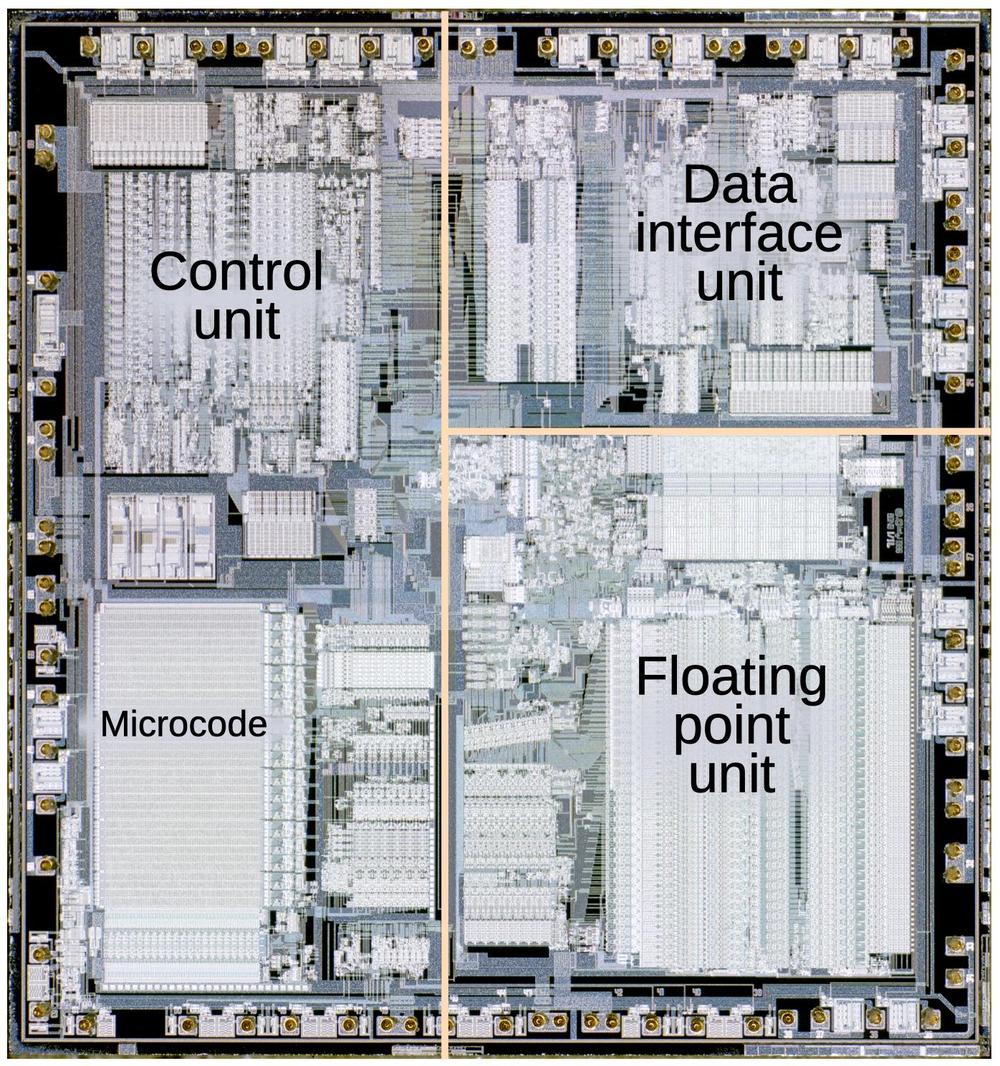
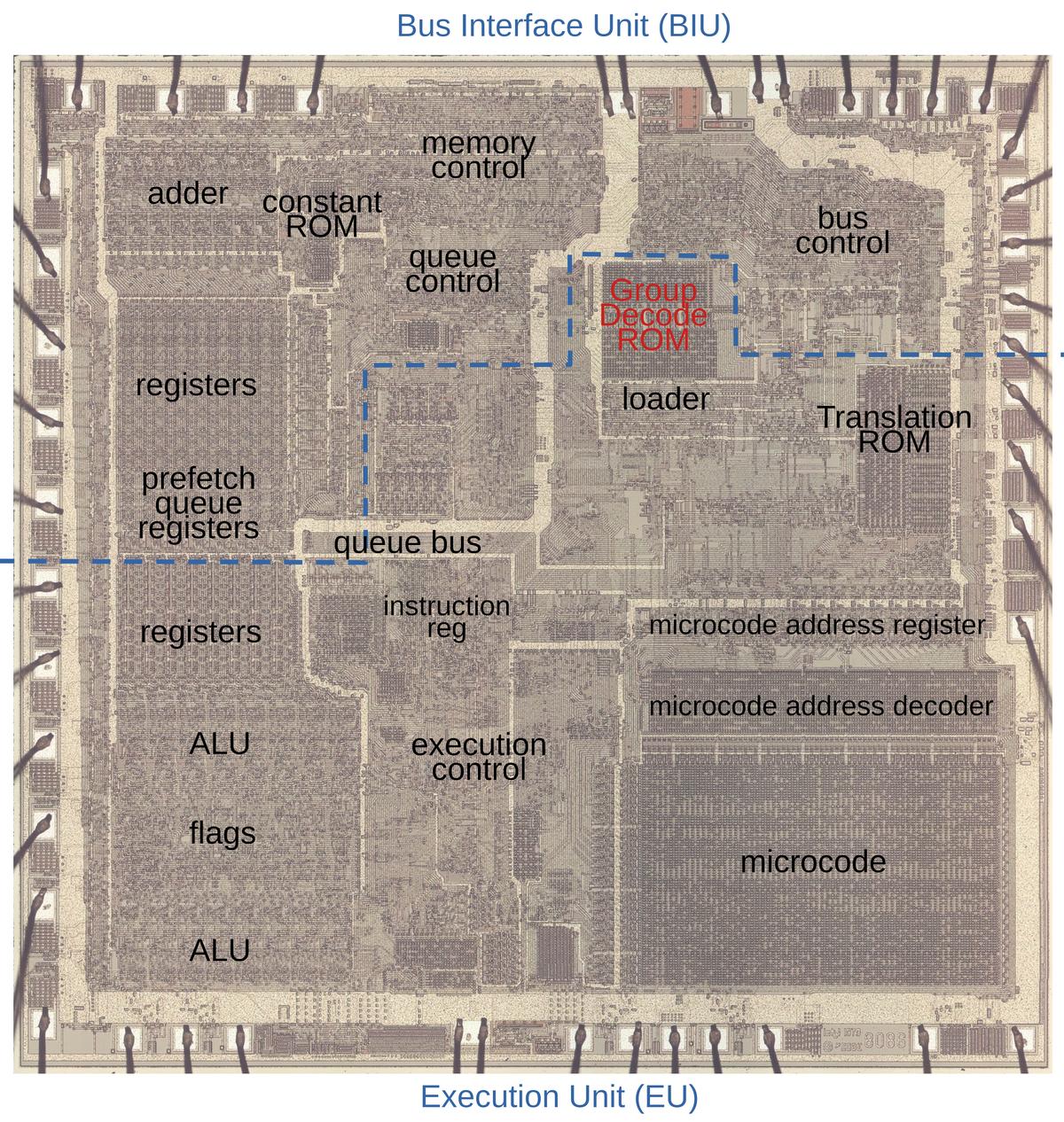
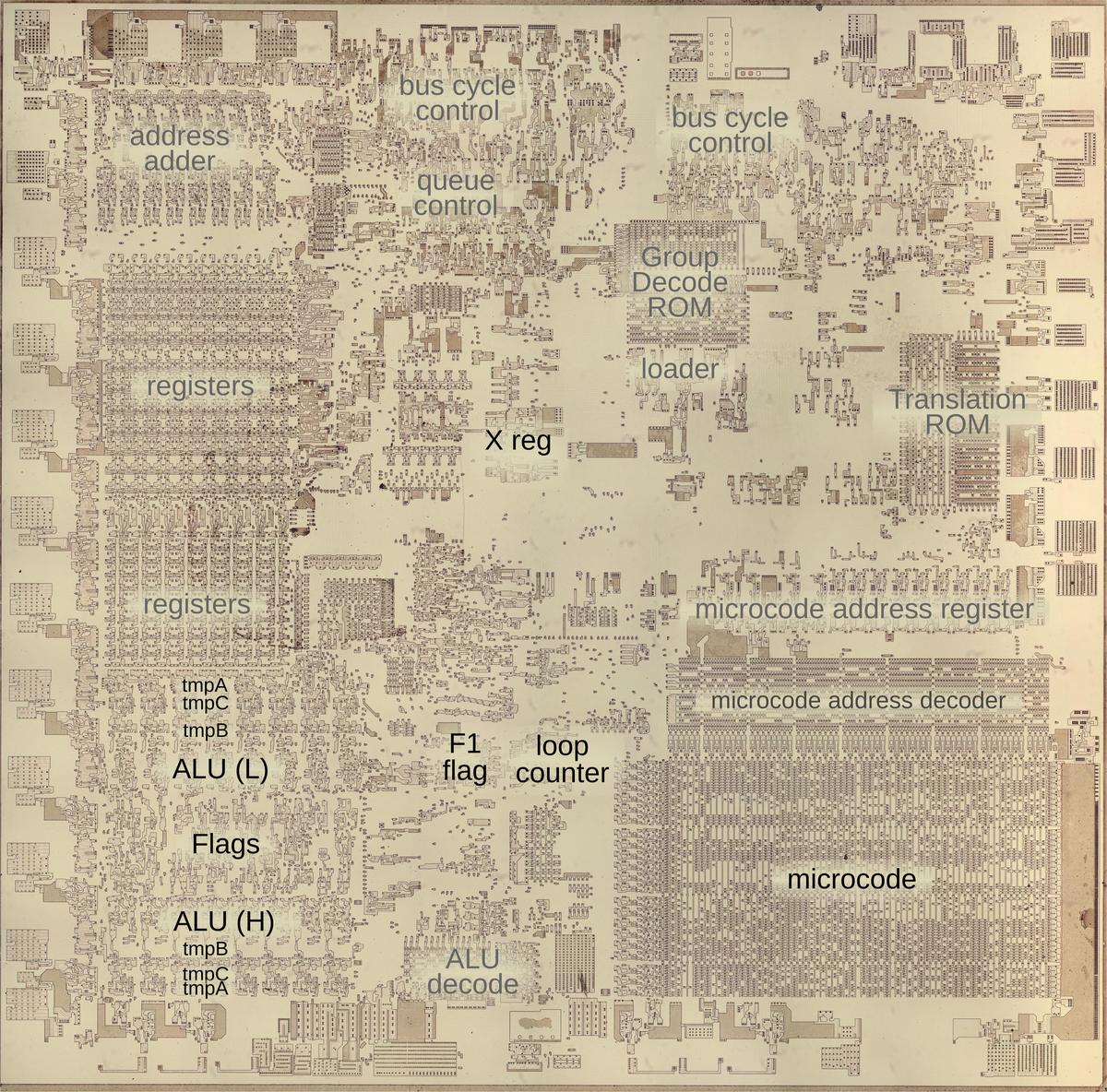
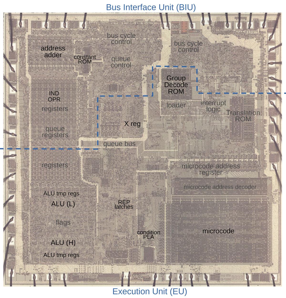
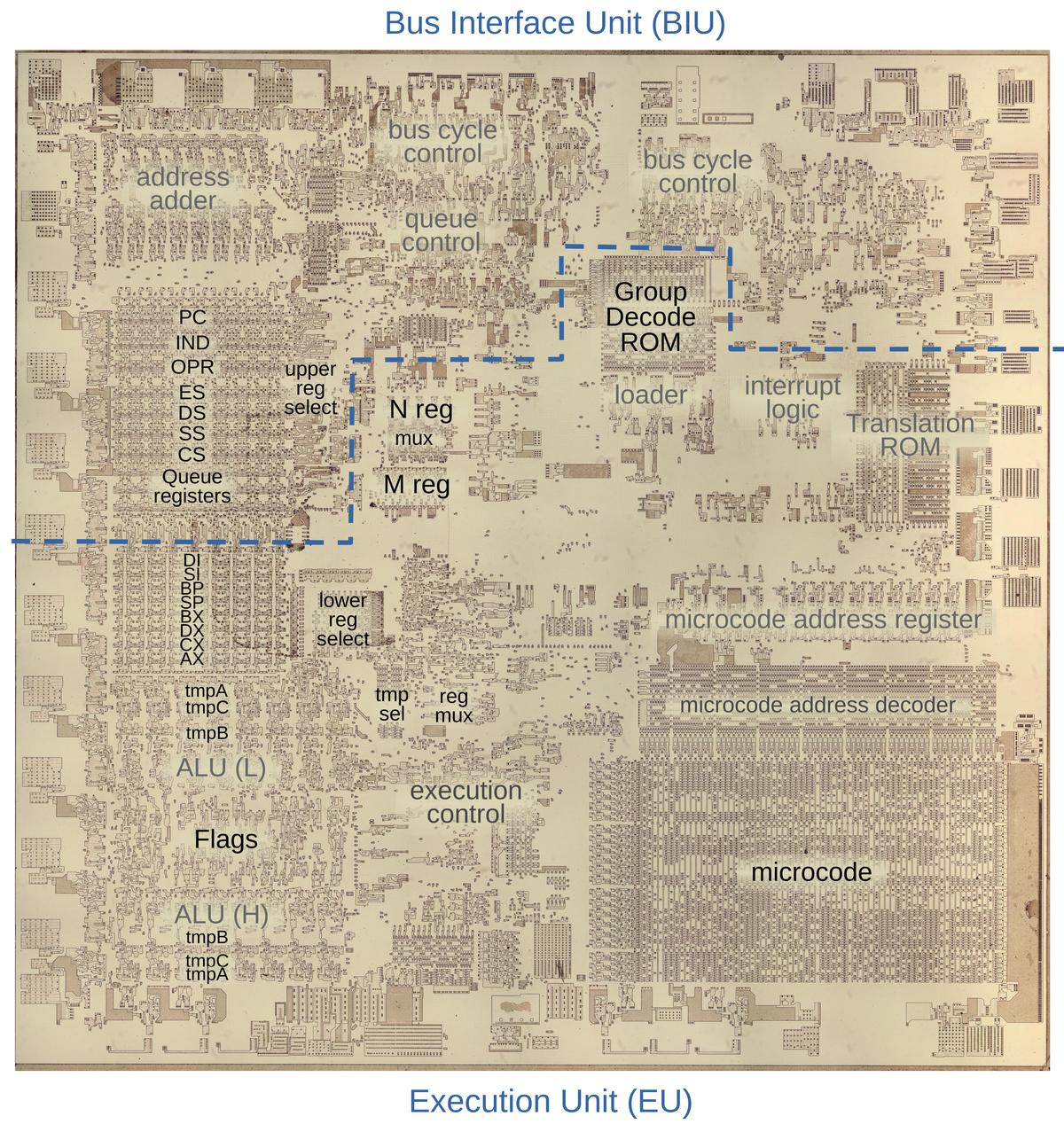
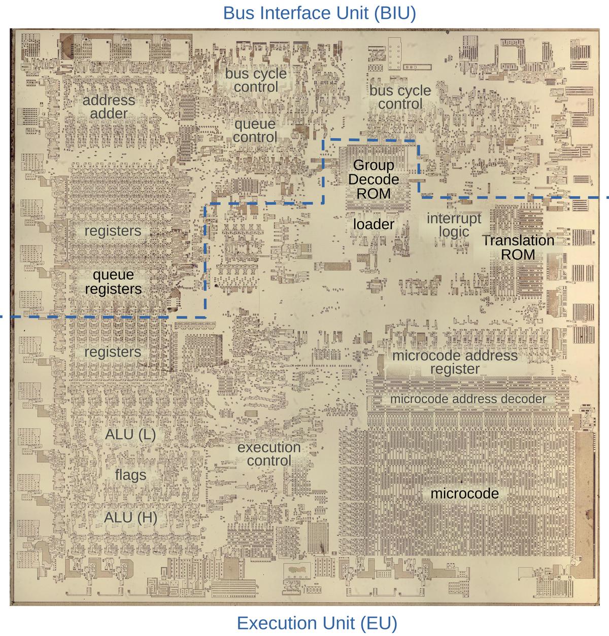
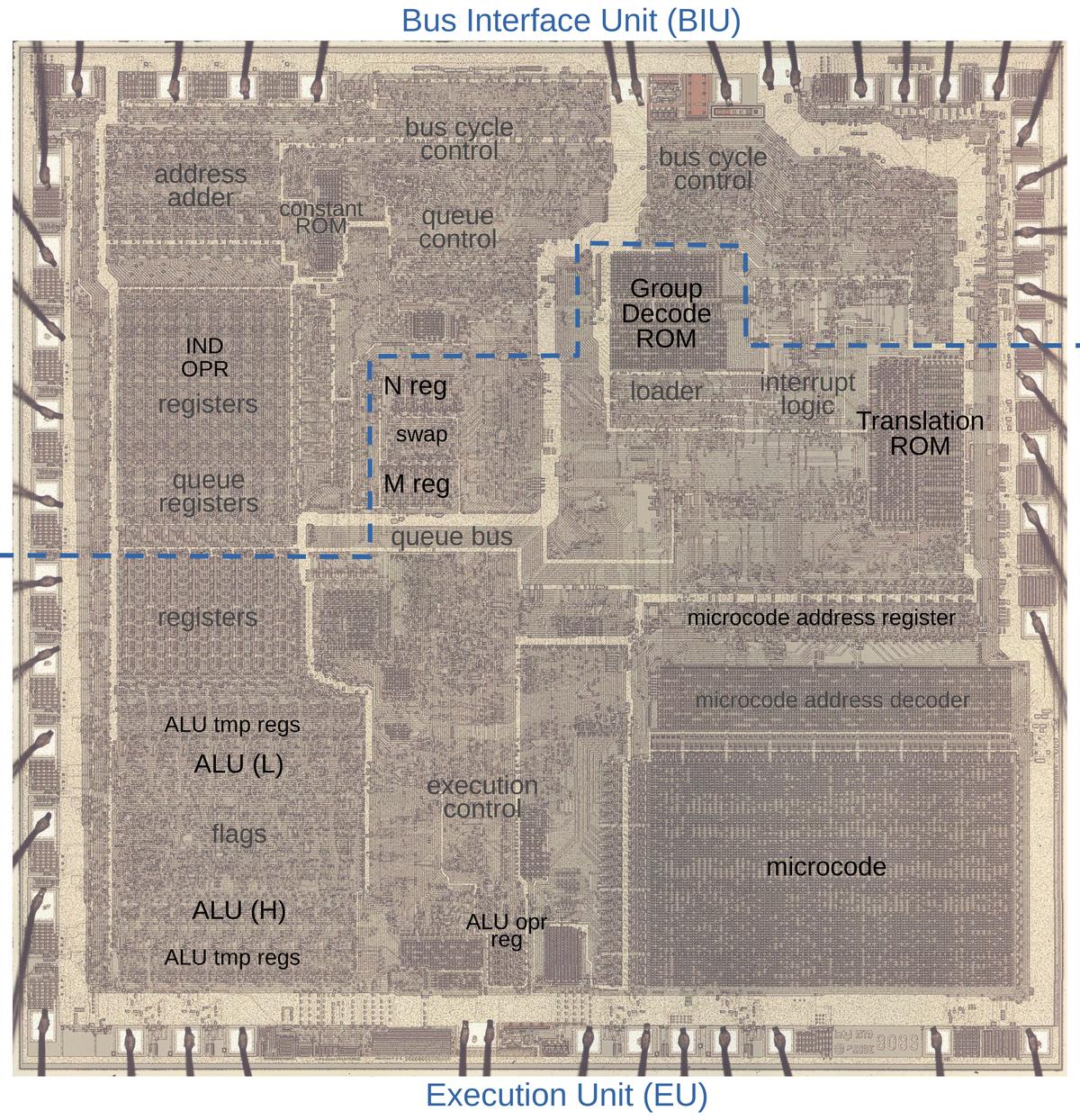
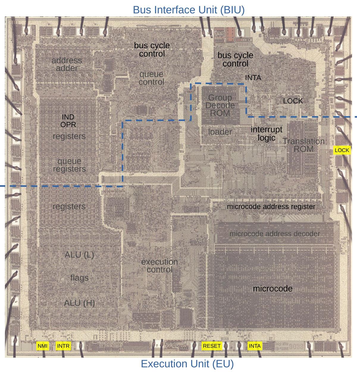
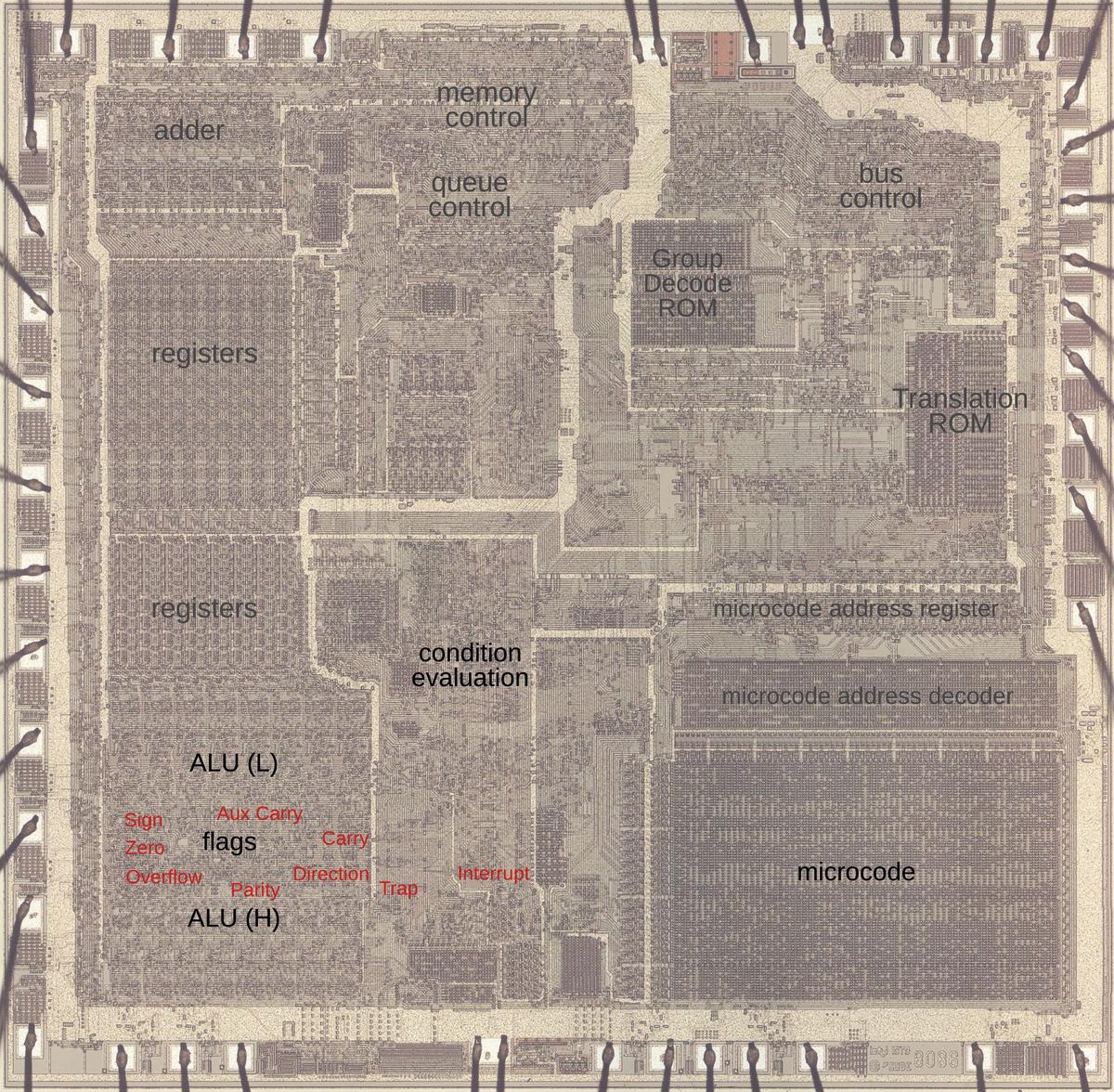
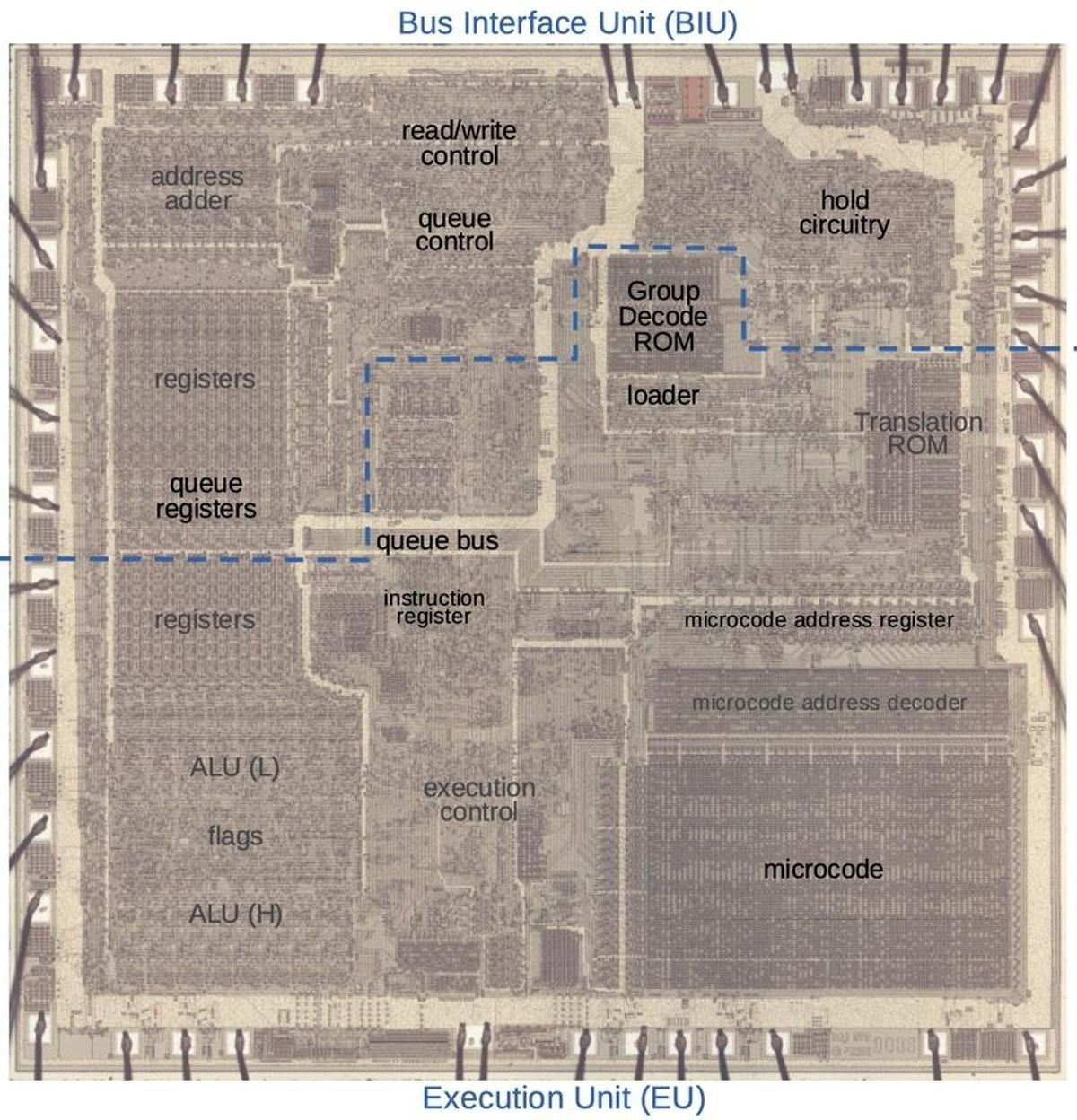
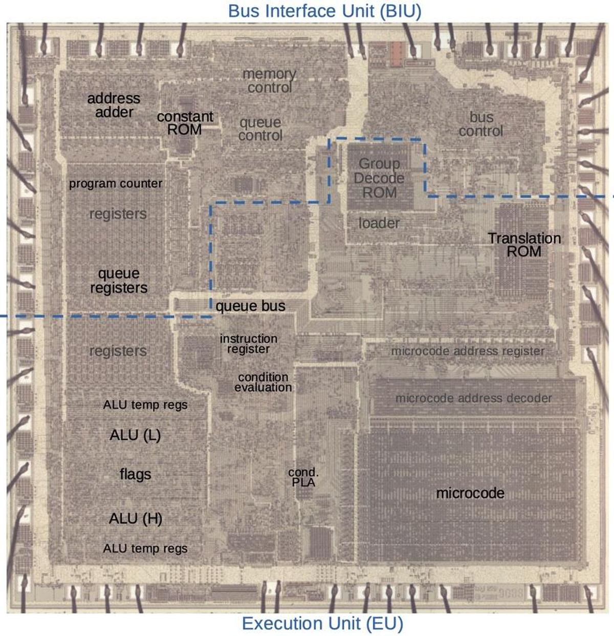
The photo below shows the 8086 die under a microscope, with the important functional blocks labeled. The metal layer is visible, while the underlying silicon and polysilicon wiring is mostly hidden. The microcode ROM and the microcode address decoder are in the lower right. The Group Decode ROM (upper center) is also important, as it performs the first step of instruction decoding.
https://static.righto.com/images/8086-ad-undoc/die-labeled.jpg">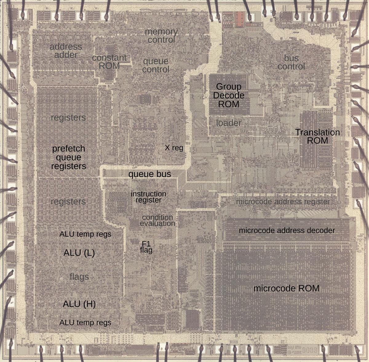
Microcode and 8086 instruction decoding
You might think that machine instructions are the basic steps that a computer performs. However, instructions usually require multiple steps inside the processor. One way of expressing these multiple steps is through microcode, a technique dating back to 1951. To execute a machine instruction, the computer internally executes several simpler micro-instructions, specified by the microcode. In other words, microcode forms nother layer between the machine instructions and the hardware. The main advantage of microcode is that it turns the processor's control logic into a programming task instead of a difficult logic design task.
The 8086's https://www.righto.com/2022/11/how-8086-processors-microcode-engine.html">microcode ROM holds 512 micro-instructions, each 21 bits wide. Each micro-instruction performs two actions in parallel. First is a move between a source and a destination, typically registers. Second is an operation that can range from an arithmetic (ALU) operation to a memory access. The diagram below shows the structure of a 21-bit micro-instruction, divided into six types.
https://static.righto.com/images/8086-ad-undoc/microcode-format.jpg">
When executing a machine instruction, the 8086 performs a decoding step.
Although the 8086 is a 16-bit processor, its instructions are based on bytes. In most cases, the first byte specifies the
opcode, which may be followed by additional instruction bytes.
In other cases, the byte is a "prefix" byte, which changes the behavior of the following instruction.
The first byte is analyzed
by something called the https://www.righto.com/2023/05/8086-processor-group-decode-rom.html">Group Decode ROM.
This circuit categorizes the first byte of the instruction into about 35 categories that control how the instruction is
decoded and executed.
One category is "1-byte logic"; this indicates a one-byte instruction or prefix that is simple and implemented by logic circuitry in the 8086.
For instructions in this category, microcode is not involved while
the remaining instructions are implemented in microcode.
Many of these instructions are in the "two-byte ROM" category indicating that the instruction has a second byte
that also needs to be decoded by microcode.
This second byte, called the ModR/M byte, specifies that memory addressing mode or registers that the instruction uses.
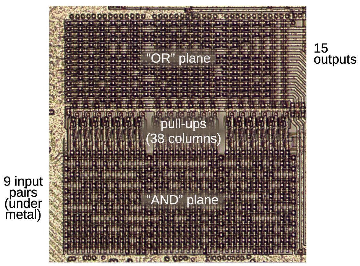
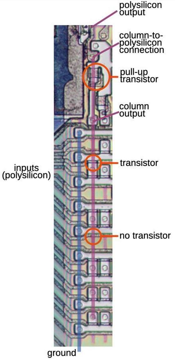
The next step is the microcode's address decoder circuit, which determines where to start executing microcode based on the opcode. Conceptually, you can think of the microcode as stored in a ROM, indexed by the instruction opcode and a few sequence bits. However, since many instructions can use the same microcode, it would be inefficient to store duplicate copies of these routines. Instead, the microcode address decoder permits multiple instructions to reference the same entries in the ROM. This decoding circuitry is similar to a PLA (Programmable Logic Array) so it matches bit patterns to determine a particular starting point. This turns out to be important for undocumented instructions since undocumented instructions often match the pattern for a "real" instruction, making the undocumented instruction an alias.
The 8086 has several internal registers that are invisible to the programmer but are used by the microcode.
Memory accesses use the Indirect (IND) and Operand (OPR) registers; the IND register holds the address in the segment,
while the OPR register holds the data value that is read or written.
Although these registers are normally not accessible by the programmer, some undocumented instructions provide access to these registers, as will be described later.
The Arithmetic/Logic Unit (ALU) performs arithmetic, logical, and shift operations in the 8086.
The ALU uses three internal registers: tmpA, tmpB, and tmpC. An ALU operation requires two micro-instructions.
The first micro-instruction specifies the operation (such as ADD) and the temporary register that holds one argument (e.g. tmpA);
the second argument is always in tmpB.
A following micro-instruction can access the ALU result through the pseudo-register Σ (sigma).
The ModR/M byte
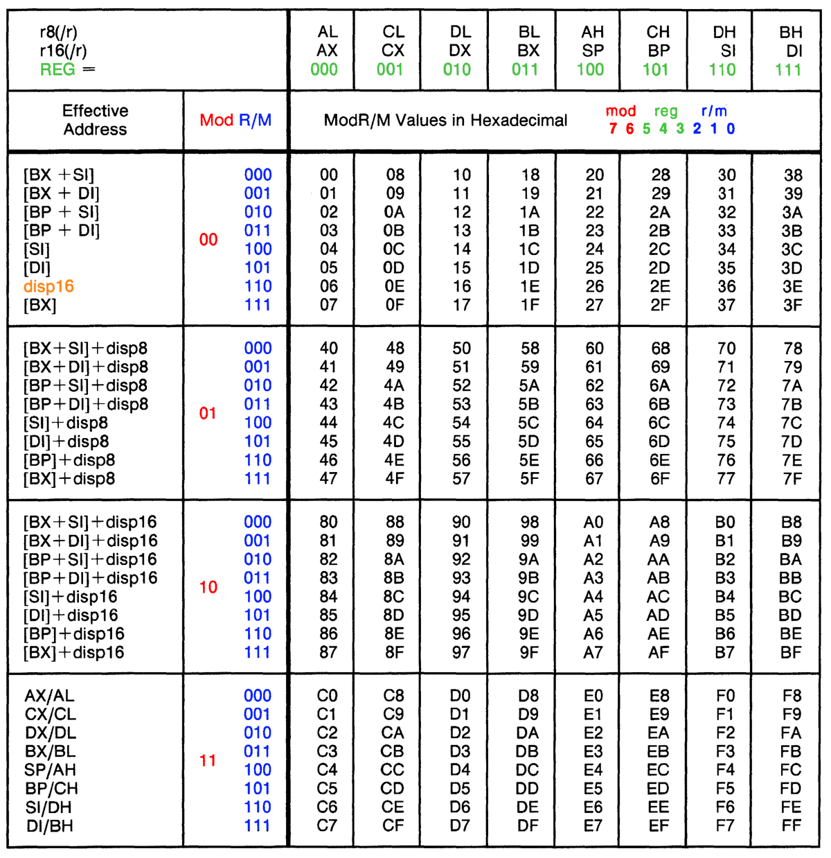
A fundamental part of the 8086 instruction format is the ModR/M byte, a byte that specifies addressing for many instructions. The 8086 has a variety of addressing modes, so the ModR/M byte is somewhat complicated. Normally it specifies one memory address and one register. The memory address is specified through one of eight addressing modes (below) along with an optional 8- or 16-bit displacement in the instruction. Instead of a memory address, the ModR/M byte can also specify a second register. For a few opcodes, the ModR/M byte selects what instruction to execute rather than a register.
https://static.righto.com/images/8086-ad-undoc/modrm.png">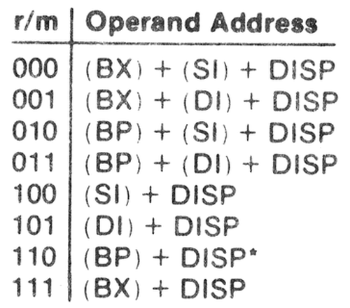
The implementation of the ModR/M byte plays an important role in the behavior of undocumented instructions.
Support for this byte is implemented in both microcode and hardware.
The various memory address modes above are implemented by microcode subroutines, which compute the appropriate memory address and
perform a read if necessary.
The subroutine leaves the memory address in the IND register, and if a read is performed, the value is in the OPR register.
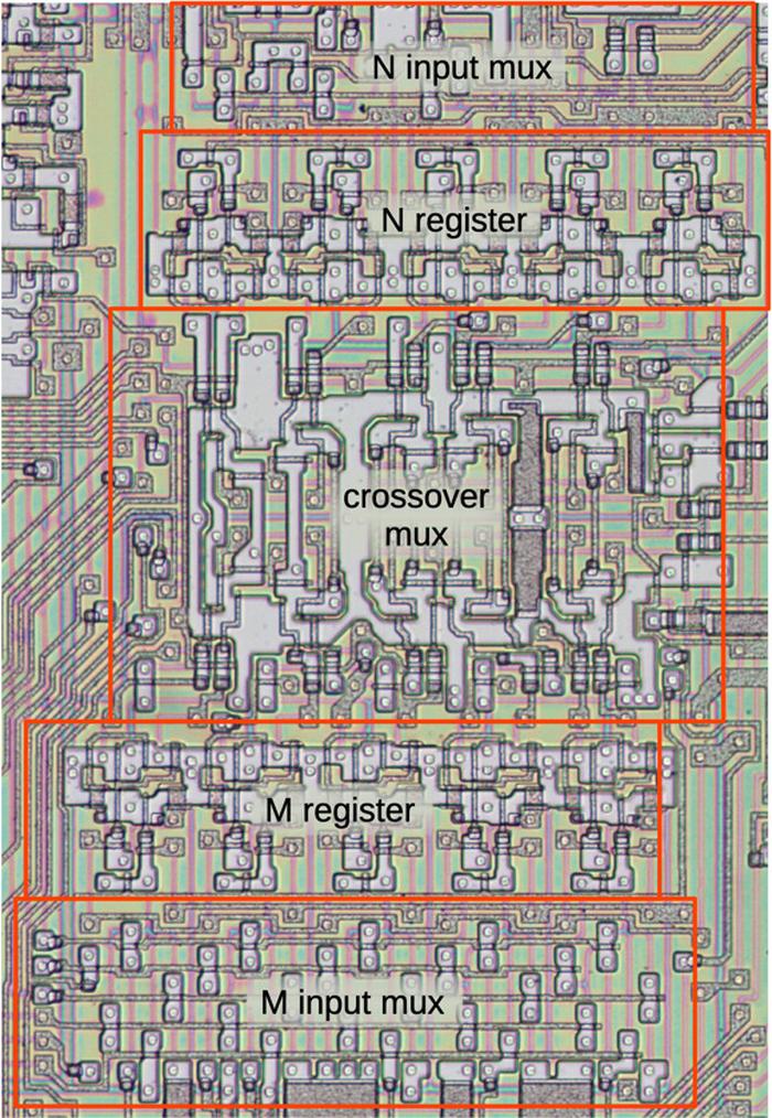
The hardware hides the ModR/M byte's selection of memory versus register, by making the value available through the pseudo-register M, while the second register is available through N.
Thus, the microcode for an instruction doesn't need to know if the value was in memory or a register, or which register was selected.
The Group Decode ROM examines the first byte of the instruction to determine if a ModR/M byte is present, and if a read
is required.
If the ModR/M byte specifies memory, the Translation ROM determines which micro-subroutines to call before handling the
instruction itself.
For more on the ModR/M byte, see my post on https://www.righto.com/2023/02/8086-modrm-addressing.html">Reverse-engineering the ModR/M addressing microcode.
Holes in the opcode table
The first byte of the instruction is a value from 00 to FF in hex.
Almost all of these opcode values correspond to documented 8086 instructions, but there are a few exceptions, "holes" in the opcode table.
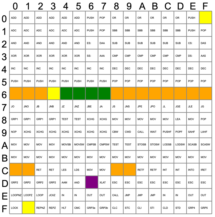
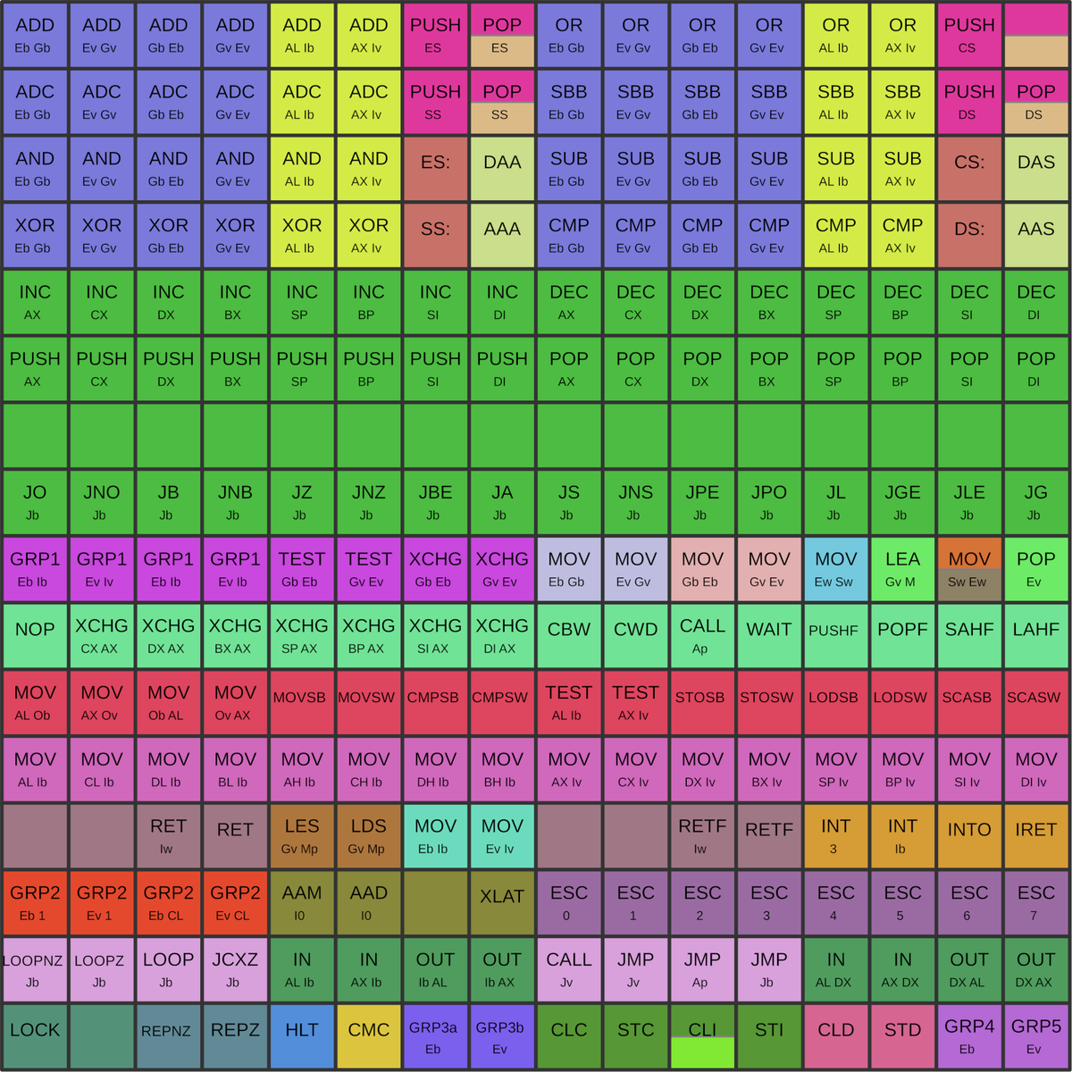
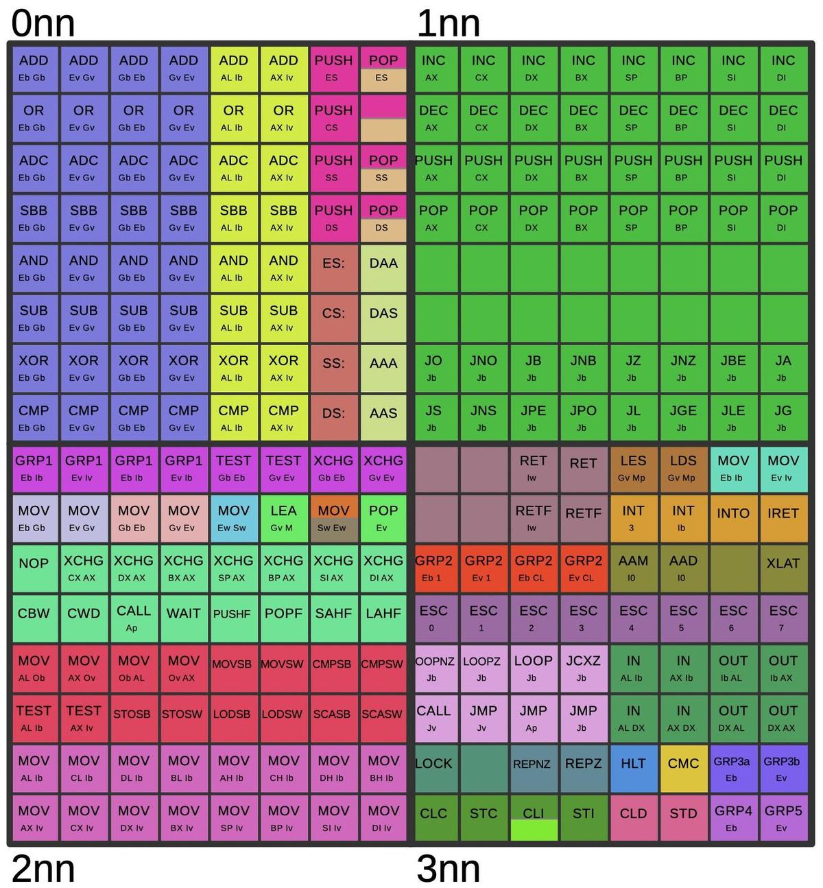
The table below shows the 256 first-byte opcodes for the 8086, from hex 00 to FF. Valid opcodes for the 8086 are in white;
the colored opcodes are undefined and interesting to examine.
Orange, yellow, and green opcodes were given meaning in the 80186, 80286, and 80386 respectively.
The purple opcode is unusual: it was implemented in the 8086 and later processors but not documented.2
In this section, I'll examine the microcode for these opcode holes.
D6: SALC
The opcode D6 (purple above) performs a well-known but undocumented operation that is typically called SALC, for Set AL to Carry.
This instruction sets the AL register to 0 if the carry flag is 0, and sets the AL register to FF if the carry flag is 1.
The curious thing about this undocumented instruction is that it exists in all x86 CPUs, but Intel didn't mention it until 2017.
Intel probably put this instruction into the processor deliberately as a copyright trap.
The idea is that if a company created a copy of the 8086 processor and the processor included the SALC instruction, this
would prove that the company had copied Intel's microcode and thus had potentially violated Intel's copyright on the microcode.
This came to light when NEC created improved versions of the 8086, the NEC V20 and V30 microprocessors, and was sued by Intel.
Intel analyzed NEC's microcode but was disappointed to find that NEC's chip did not include the hidden instruction, showing
that NEC hadn't copied the microcode.3
Although a Federal judge ruled in 1989 that NEC hadn't infringed
Intel's copyright, the 5-year trial ruined NEC's market momentum.
The SALC instruction is implemented with three micro-instructions, shown below.4
The first micro-instruction jumps if the carry (CY) is set.
If not, the next instruction moves 0 to the AL register. RNI (Run Next Instruction) ends the microcode execution
causing the next machine instruction to run.
If the carry was set, all-ones (i.e. FF hex) is moved to the AL register and RNI ends the microcode sequence.
           JMPS CY 2 SALC: jump on carry
ZERO → AL  RNI       Move 0 to AL, run next instruction
ONES → AL  RNI       2:Move FF to AL, run next instruction
0F: POP CS
The 0F opcode is the first hole in the opcode table.
The 8086 has instructions to push and pop the four segment registers, except opcode 0F is undefined where POP CS should be.
This opcode performs POP CS successfully, so the question is why is it undefined?
The reason is that POP CS is essentially useless and doesn't do what you'd expect, so Intel figured it was best not
to document it.
To understand why POP CS is useless, I need to step back and explain the 8086's segment registers.
The 8086 has a 20-bit address space, but 16-bit registers.
To make this work, the 8086 has the concept of segments: memory is accessed in 64K chunks called segments, which are positioned
in the 1-megabyte address space.
Specifically, there are four segments: Code Segment, Stack Segment, Data Segment, and Extra Segment,
with four segment registers that define the start of the segment: CS, SS, DS, and ES.
An inconvenient part of segment addressing is that if you want to access more than 64K, you need to change the segment register.
So you might push the data segment register, change it temporarily so you can access a new part of memory, and then pop the old data segment
register value off the stack.
This would use the PUSH DS and POP DS instructions.
But why not POP CS?
The 8086 executes code from the code segment, with the instruction pointer (IP) tracking the location in the code segment.
The main problem with POP CS is that it changes the code segment, but not the instruction pointer, so now you are executing
code at the old offset in a new segment.
Unless you line up your code extremely carefully, the result is that you're jumping to an unexpected place in memory.
(Normally, you want to change CS and the instruction pointer at the same time, using a CALL or JMP instruction.)
The second problem with POP CS is prefetching.
For efficiency, the 8086 prefetches instructions before they are needed, storing them in an 8-byte prefetch queue.
When you perform a jump, for instance, the microcode flushes the prefetch queue so execution will continue with the
new instructions, rather than the old instructions.
However, the instructions that pop a segment register don't flush the prefetch buffer.
Thus, POP CS not only jumps to an unexpected location in memory, but it will execute an unpredictable number of instructions
from the old code path.
The POP segment register microcode below packs a lot into three micro-instructions.
The first micro-instruction pops a value from the stack.
Specifically, it moves the stack pointer (SP) to the Indirect (IND) register.
The Indirect register is an internal register, invisible to the programmer, that holds the address offset for memory
accesses.
The first micro-instruction also performs a memory read (R) from the stack segment (SS) and then increments IND
by 2 (P2, plus 2).
The second micro-instruction moves IND to the stack pointer, updating the stack pointer with the new value.
It also tells the microcode engine that this micro-instruction is the next-to-last (NXT) and the next machine instruction
can be started.
The final micro-instruction moves the value read from memory to the appropriate segment register and runs the next instruction.
Specifically, reads and writes put data in the internal OPR (Operand) register.
The hardware uses the register N to indicate the register specified by the instruction.
That is, the value will be stored in the CS, DS, ES, or SS register, depending on the bit pattern in the instruction.
Thus, the same microcode works for all four segment registers.
This is why POP CS works even though POP CS wasn't explicitly implemented in the microcode; it uses the common code.
SP → IND  R SS,P2 POP sr: read from stack, compute IND plus 2
IND → SP  NXT     Put updated value in SP, start next instruction.
OPR → N   RNI     Put stack value in specified segment register
But why does POP CS run this microcode in the first place?
The microcode to execute is selected based on the instruction, but multiple instructions can execute the same microcode.
You can think of the address decoder as pattern-matching on the instruction's bit patterns, where some of the bits can be ignored.
In this case, the POP sr microcode above is run by any instruction with the bit pattern 000??111, where a question mark
can be either a 0 or a 1.
You can verify that this pattern matches POP ES (07), POP SS (17), and POP DS (1F).
However, it also matches 0F, which is why the 0F opcode runs the above microcode and performs POP CS.
In other words, to make 0F do something other than POP CS would require additional circuitry, so it was easier to
leave the action implemented but undocumented.
60-6F: conditional jumps
One whole row of the opcode table is unused: values 60 to 6F.
These opcodes simply act the same as 70 to 7F, the conditional jump instructions.
The conditional jumps use the following microcode.
It fetches the jump offset from the instruction prefetch queue (Q) and puts the value into the ALU's tmpBL register,
the low byte of the tmpB register.
It tests the condition in the instruction (XC) and jumps to the RELJMP micro-subroutine if satisfied.
The RELJMP code (not shown) updates the program counter to perform the jump.
Q → tmpBL                Jcond cb: Get offset from prefetch queue
           JMP XC RELJMP Test condition, if true jump to RELJMP routine
           RNI           No jump: run next instruction
This code is executed for any instruction matching the bit pattern 011?????, i.e. anything from 60 to 7F.
The condition is specified by the four low bits of the instruction.
The result is that any instruction 60-6F is an alias for the corresponding conditional jump 70-7F.
C0, C8: RET/RETF imm
These undocumented opcodes act like a return instruction, specifically RET imm16 (source).
Specifically, the instruction C0 is the same as C2, near return, while C8 is the same as CA, far return.
The microcode below is executed for the instruction bits 1100?0?0, so it is executed for C0, C2, C8, and CA.
It gets two bytes from the instruction prefetch queue (Q) and puts them in the tmpA register.
Next, it calls FARRET, which performs either a near return (popping PC from the stack) or a far return (popping PC and CS
from the stack). Finally, it adds the original argument to the SP, equivalent to popping that many bytes.
Q → tmpAL    ADD tmpA    RET/RETF iw: Get word from prefetch, set up ADD
Q → tmpAH    CALL FARRET Call Far Return micro-subroutine
IND → tmpB               Move SP (in IND) to tmpB for ADD
Σ → SP       RNI         Put sum in Stack Pointer, end
One tricky part is that the FARRET micro-subroutine examines bit 3 of the instruction to determine whether it does a near
return or a far return.
This is why documented instruction C2 is a near return and CA is a far return.
Since C0 and C8 run the same microcode, they will perform the same actions, a near return and a far return respectively.
C1: RET
The undocumented C1 opcode is identical to the documented C3, near return instruction.
The microcode below is executed for instruction bits 110000?1, i.e. C1 and C3.
The first micro-instruction reads from the Stack Pointer, incrementing IND by 2.
Prefetching is suspended and the prefetch queue is flushed, since execution will continue at a new location.
The Program Counter is updated with the value from the stack, read into the OPR register.
Finally, the updated address is put in the Stack Pointer and execution ends.
SP → IND  R SS,P2  RET:  Read from stack, increment by 2
          SUSP     Suspend prefetching
OPR → PC  FLUSH    Update PC from stack, flush prefetch queue
IND → SP  RNI      Update SP, run next instruction
C9: RET
The undocumented C9 opcode is identical to the documented CB, far return instruction.
This microcode is executed for instruction bits 110010?1, i.e. C9 and CB, so C9 is identical to CB.
The microcode below simply calls the FARRET micro-subroutine to pop the Program Counter and CS register.
Then the new value is stored into the Stack Pointer.
One subtlety is that FARRET looks at bit 3 of the instruction to switch between a near return and a far return, as
described earlier.
Since C9 and CB both have bit 3 set, they both perform a far return.
          CALL FARRET  RETF: call FARRET routine
IND → SP  RNI          Update stack pointer, run next instruction
F1: LOCK prefix
The final hole in the opcode table is F1.
This opcode is different because it is implemented in logic rather than microcode.
The Group Decode ROM indicates that F1 is a prefix, one-byte logic, and LOCK.
The Group Decode outputs are the same as F0, so F1 also acts as a LOCK prefix.
Holes in two-byte opcodes
For most of the 8086 instructions, the first byte specifies the instruction.
However, the 8086 has a few instructions where the second byte specifies the instruction: the reg field of the ModR/M byte provides an opcode extension that selects the instruction.5
These fall into four categories which Intel labeled "Immed", "Shift", "Group 1", and "Group 2", corresponding to opcodes 80-83, D0-D3,
F6-F7, and FE-FF.
The table below shows how the second byte selects the instruction.
Note that "Shift", "Group 1", and "Group 2" all have gaps, resulting in undocumented values.
These sets of instructions are implemented in two completely different ways.
The "Immed" and "Shift" instructions run microcode in the standard way, selected by the first byte.
For a typical arithmetic/logic instruction such as ADD, bits 5-3 of the first instruction byte are latched into the X register to indicate
which ALU operation to perform.
The microcode specifies a generic ALU operation, while the X register controls whether the operation is an ADD, SUB, XOR, or
so forth.
However, the Group Decode ROM indicates that for the special "Immed" and "Shift" instructions, the X register latches the bits
from the second byte.
Thus, when the microcode executes a generic ALU operation, it ends up with the one specified in the second byte.6
The "Group 1" and "Group 2" instructions (F0-F1, FE-FF), however, run different microcode for each instruction.
Bits 5-3 of the second byte replace bits 2-0 of the instruction before executing the microcode.
Thus, F0 and F1 act as if they are opcodes in the range F0-F7, while FE and FF act as if they are opcodes in the range F8-FF.
Thus, each instruction specified by the second byte can have its own microcode, unlike the "Immed" and "Shift" instructions.
The trick that makes this work is that all the "real" opcodes in the range F0-FF are implemented in logic, not microcode,
so there are no collisions.
The hole in "Shift": SETMO, D0..D3/6
There is a "hole" in the list of shift operations when the second byte has the bits 110 (6).
(This is typically expressed as D0/6 and so forth; the value after the slash is the opcode-selection bits in the ModR/M byte.)
Internally, this value selects the ALU's SETMO (Set Minus One) operation, which simply returns FF or FFFF, for a byte or word operation respectively.7
The microcode below is executed for 1101000? bit patterns patterns (D0 and D1).
The first instruction gets the value from the M register and sets up the ALU to do whatever operation was
specified in the instruction (indicated by XI).
Thus, the same microcode is used for all the "Shift" instructions, including SETMO.
The result is written back to M. If no writeback to memory is required (NWB), then RNI runs the next instruction, ending
the microcode sequence.
However, if the result is going to memory, then the last line writes the value to memory.
M → tmpB  XI tmpB, NXT  rot rm, 1: get argument, set up ALU
Σ → M     NWB,RNI F     Store result, maybe run next instruction
          W DS,P0 RNI   Write result to memory
The D2 and D3 instructions (1101001?) perform a variable number of shifts, specified by the CL register, so they use different microcode (below).
This microcode loops the number of times specified by CL, but the control flow is a bit tricky to avoid shifting if
the intial counter value is 0.
The code sets up the ALU to pass the counter (in tmpA) unmodified the first time (PASS) and jumps to 4, which
updates the counter and sets up the ALU for the shift operation (XI).
If the counter is not zero, it jumps back to 3, which performs the previously-specified shift and sets up
the ALU to decrement the counter (DEC).
This time, the code at 4 decrements the counter.
The loop continues until the counter reaches zero. The microcode stores the result as in the previous microcode.
ZERO → tmpA               rot rm,CL: 0 to tmpA
CX → tmpAL   PASS tmpA    Get count to tmpAL, set up ALU to pass through
M → tmpB     JMPS 4       Get value, jump to loop (4)
Σ → tmpB     DEC tmpA F   3: Update result, set up decrement of count
Σ → tmpA     XI tmpB      4: update count in tmpA, set up ALU
             JMPS NZ 3    Loop if count not zero
tmpB → M     NWB,RNI      Store result, maybe run next instruction
             W DS,P0 RNI  Write result to memory
The hole in "group 1": TEST, F6/1 and F7/1
The F6 and F7 opcodes are in "group 1", with the specific instruction specified by bits 5-3 of the second byte.
The second-byte table showed a hole for the 001 bit sequence.
As explained earlier, these bits replace the low-order bits of the instruction, so F6 with 001 is processed as if it were
the opcode F1.
The microcode below matches against instruction bits 1111000?, so F6/1 and F7/1 have the same effect as F6/0 and F7/1 respectively,
that is, the byte and word TEST instructions.
The microcode below gets one or two bytes from the prefetch queue (Q); the L8 condition tests if the operation is
an 8-bit (i.e. byte) operation and skips the second micro-instruction.
The third micro-instruction ANDs the argument and the fetched value.
The condition flags (F) are set based on the result, but the result itself is discarded.
Thus, the TEST instruction tests a value against a mask, seeing if any bits are set.
Q → tmpBL    JMPS L8 2     TEST rm,i: Get byte, jump if operation length = 8
Q → tmpBH                  Get second byte from the prefetch queue
M → tmpA     AND tmpA, NXT 2: Get argument, AND with fetched value
Σ → no dest  RNI F         Discard result but set flags.
I explained the processing of these "Group 3" instructions in more detail in my microcode article.
The hole in "group 2": PUSH, FE/7 and FF/7
The FE and FF opcodes are in "group 2", which has a hole for the 111 bit sequence in the second byte.
After replacement, this will be processed as the FF opcode, which matches the pattern 1111111?.
In other words, the instruction will be processed the same as the 110 bit pattern, which is PUSH.
The microcode gets the Stack Pointer, sets up the ALU to decrement it by 2.
The new value is written to SP and IND. Finally, the register value is written to stack memory.
SP → tmpA  DEC2 tmpA   PUSH rm: set up decrement SP by 2
Σ → IND                Decremented SP to IND
Σ → SP                 Decremented SP to SP
M → OPR    W SS,P0 RNI Write the value to memory, done
82 and 83 "Immed" group
Opcodes 80-83 are the "Immed" group, performing one of eight arithmetic operations, specified in the ModR/M byte.
The four opcodes differ in the size of the values: opcode 80 applies an 8-bit immediate value to an 8-bit register, 81 applies a 16-bit
value to a 16-bit register, 82 applies an 8-bit value to an 8-bit register, and 83 applies an 8-bit value to a 16-bit register.
The opcode 82 has the strange situation that some sources say it is undocumented, but it shows up in some Intel documentation as a valid bit combination (e.g. below).
Note that 80 and 82 have the 8-bit to 8-bit action, so the 82 opcode is redundant.
The microcode below is used for all four opcodes.
If the ModR/M byte specifies memory, the appropriate micro-subroutine is called to compute the effective address in IND,
and fetch the byte or word into OPR.
The first two instructions below get the two immediate data bytes from the prefetch queue; for an 8-bit operation, the second byte
is skipped.
Next, the second argument M is loaded into tmpA and the desired ALU operation (XI) is configured.
The result Σ is stored into the specified register M and the operation may terminate with RNI.
But if the ModR/M byte specified memory, the following write micro-operation saves the value to memory.
Q → tmpBL  JMPS L8 2    alu rm,i: get byte, test if 8-bit op
Q → tmpBH               Maybe get second byte
M → tmpA   XI tmpA, NXT 2:
Σ → M      NWB,RNI F    Save result, update flags, done if no memory writeback
           W DS,P0 RNI  Write result to memory if needed
The tricky part of this is the L8 condition, which tests if the operation is 8-bit.
You might think that bit 0 acts as the byte/word bit in a nice, orthogonal way, but the 8086 has a bunch of special cases.
Bit 0 of the instruction typically selects between a byte and a word operation, but there are a bunch of special cases.
The Group Decode ROM creates a signal indicating if bit 0 should be used as the byte/word bit.
But it generates a second signal indicating that an instruction should be forced to operate on bytes, for instructions
such as DAA and XLAT.
Another Group Decode ROM signal indicates that bit 3 of the instruction should select byte or word; this
is used for the MOV instructions with opcodes Bx.
Yet another Group Decode ROM signal indicates that inverted bit 1 of the instruction should select byte or word;
this is used for a few opcodes, including 80-87.
The important thing here is that for the opcodes under discussion (80-83), the L8 micro-condition uses both bits 0 and 1
to determine if the instruction is 8 bits or not.
The result is that only opcode 81 is considered 16-bit by the L8 test, so it is the only one that uses two immediate bytes
from the instruction.
However, the register operations use only bit 0 to select a byte or word transfer.
The result is that opcode 83 has the unusual behavior of using an 8-bit immediate operand with a 16-bit register.
In this case, the 8-bit value is sign-extended to form a 16-bit value. That is, the top bit of the 8-bit value fills
the entire upper half of the 16-bit value,
converting an 8-bit signed value to a 16-bit signed value (e.g. -1 is FF, which becomes FFFF).
This makes sense for arithmetic operations, but not much sense for logical operations.
Intel documentation is inconsistent about which opcodes are listed for which instructions.
Intel opcode maps generally define opcodes 80-83.
However, lists of specific instructions show opcodes 80, 81, and 83 for arithmetic operations but only 80 and 81 for logical operations.8
That is, Intel omits the redundant 82 opcode as well as omitting logic operations that perform sign-extension (83).
More FE holes
For the "group 2" instructions, the FE opcode performs a byte operation while FF performs a word operation.
Many of these operations don't make sense for bytes: CALL, JMP, and PUSH.
(The only instructions supported for FE are INC and DEC.) But what happens if you use the unsupported instructions?
The remainder of this section examines those cases and shows that the results are not useful.
CALL: FE/2
This instruction performs an indirect subroutine call within a segment, reading the target address from the memory location specified by the ModR/M byte.
The microcode below is a bit convoluted because the code falls through into the shared NEARCALL routine, so there is
some unnecessary register movement.
Before this microcode executes, the appropriate ModR/M micro-subroutine will read the target address from memory.
The code below copies the destination address from M to tmpB and stores it into the PC later in the code
to transfer execution.
The code suspends prefetching, corrects the PC to cancel the offset from prefetching, and flushes the prefetch queue.
Finally, it decrements the SP by two and writes the old PC to the stack.
M → tmpB    SUSP        CALL rm: read value, suspend prefetch
SP → IND    CORR        Get SP, correct PC
PC → OPR    DEC2 tmpC   Get PC to write, set up decrement
tmpB → PC   FLUSH       NEARCALL: Update PC, flush prefetch
IND → tmpC              Get SP to decrement
Σ → IND                 Decremented SP to IND
Σ → SP      W SS,P0 RNI Update SP, write old PC to stack
This code will mess up in two ways when executed as a byte instruction. First, when the destination address is read from memory, only a byte will be read, so the destination address will be corrupted. (I think that the behavior here depends on the bus hardware. The 8086 will ask for a byte from memory but will read the word that is placed on the bus. Thus, if memory returns a word, this part may operate correctly. The 8088's behavior will be different because of its 8-bit bus.) The second issue is writing the old PC to the stack because only a byte of the PC will be written. Thus, when the code returns from the subroutine call, the return address will be corrupt.
CALL: FE/3
This instruction performs an indirect subroutine call between segments, reading the target address from the memory location specified by the ModR/M byte.
IND → tmpC  INC2 tmpC    CALL FAR rm: set up IND+2
Σ → IND     R DS,P0      Read new CS, update IND
OPR → tmpA  DEC2 tmpC    New CS to tmpA, set up SP-2
SP → tmpC   SUSP         FARCALL: Suspend prefetch
Σ → IND     CORR         FARCALL2: Update IND, correct PC
CS → OPR    W SS,M2      Push old CS, decrement IND by 2
tmpA → CS   PASS tmpC    Update CS, set up for NEARCALL
PC → OPR    JMP NEARCALL Continue with NEARCALL
As in the previous CALL, this microcode will fail in multiple ways when executed in byte mode.
The new CS and PC addresses will be read from memory as bytes, which may or may not work.
Only a byte of the old CS and PC will be pushed to the stack.
JMP: FE/4
This instruction performs an indirect jump within a segment, reading the target address from the memory location specified by the ModR/M byte.
The microcode is short, since the ModR/M micro-subroutine does most of the work.
I believe this will have the same problem as the previous CALL instructions, that it will attempt to read a byte from
memory instead of a word.
        SUSP       JMP rm: Suspend prefetch
M → PC  FLUSH RNI  Update PC with new address, flush prefetch, done
JMP: FE/5
This instruction performs an indirect jump between segments, reading the new PC and CS values from the memory location specified by the ModR/M byte.
The ModR/M micro-subroutine reads the new PC address. This microcode increments IND and suspends prefetching.
It updates the PC, reads the new CS value from memory, and updates the CS.
As before, the reads from memory will read bytes instead of words, so this code will not meaningfully work in byte mode.
IND → tmpC  INC2 tmpC   JMP FAR rm: set up IND+2
Σ → IND     SUSP        Update IND, suspend prefetch
tmpB → PC   R DS,P0     Update PC, read new CS from memory
OPR → CS    FLUSH RNI   Update CS, flush prefetch, done
PUSH: FE/6
This instruction pushes the register or memory value specified by the ModR/M byte. It decrements the SP by 2 and then writes the value to the stack. It will write one byte to the stack but decrements the SP by 2, so one byte of old stack data will be on the stack along with the data byte.
SP → tmpA  DEC2 tmpA    PUSH rm: Set up SP decrement
Σ → IND                 Decremented value to IND
Σ → SP                  Decremented value to SP
M → OPR    W SS,P0 RNI  Write the data to the stack
Undocumented instruction values
The next category of undocumented instructions is where the first byte indicates a valid instruction, but there is something wrong with the second byte.
AAM: ASCII Adjust after Multiply
The AAM instruction is a fairly obscure one, designed to support binary-coded decimal
arithmetic (BCD).
After multiplying two BCD digits, you end up with a binary value between 0 and 81 (0×0 to 9×9).
If you want a BCD result, the AAM instruction converts this binary value to BCD, for instance splitting 81 into the
decimal digits 8 and 1, where the upper digit is 81 divided by 10, and the lower digit is 81 modulo 10.
The interesting thing about AAM is that the 2-byte instruction is D4 0A. You might notice that hex 0A is 10, and this
is not a coincidence.
There wasn't an easy way to get the value 10 in the microcode, so instead they made the instruction
provide that value in the second byte.
The undocumented (but well-known) part is that if you provide a value other than 10, the instruction will convert the binary input into
digits in that base. For example, if you provide 8 as the second byte, the instruction returns the value divided by 8
and the value modulo 8.
The microcode for AAM, below, sets up the registers. calls
the CORD (Core Division) micro-subroutine to perform the division,
and then puts the results into AH and AL.
In more detail, the CORD routine divides tmpA/tmpC by tmpB, putting the complement of the quotient in tmpC and leaving the remainder in tmpA.
(If you want to know how CORD works internally, see my division post.)
The important step is that the AAM microcode gets the divisor from the prefetch queue (Q).
After calling CORD, it sets up the ALU to perform a 1's complement of tmpC and puts the result (Σ) into AH.
It sets up the ALU to pass tmpA through unchanged, puts the result (Σ) into AL, and updates the flags accordingly (F).
Q → tmpB                    AAM: Move byte from prefetch to tmpB
ZERO → tmpA                 Move 0 to tmpA
AL → tmpC    CALL CORD      Move AL to tmpC, call CORD.
             COM1 tmpC      Set ALU to complement
Σ → AH       PASS tmpA, NXT Complement AL to AH
Σ → AL       RNI F          Pass tmpA through ALU to set flags
The interesting thing is why this code has undocumented behavior.
The 8086's microcode only has support for the constants 0 and all-1's (FF or FFFF), but the microcode needs to divide by 10.
One solution would be to implement an additional micro-instruction and more circuitry to provide the constant 10, but every
transistor was precious back then.
Instead, the designers took the approach of simply putting the number 10 as the second byte of the instruction and loading the
constant from there.
Since the AAM instruction is not used very much, making the instruction two bytes long wasn't much of a drawback.
But if you put a different number in the second byte, that's the divisor the microcode will use.
(Of course you could add circuitry to verify that the number is 10, but then the implementation is no longer simple.)
Intel could have documented the full behavior, but that creates several problems. First, Intel would be stuck supporting the full behavior into the future. Second, there are corner cases to deal with, such as divide-by-zero. Third, testing the chip would become harder because all these cases would need to be tested. Fourth, the documentation would become long and confusing. It's not surprising that Intel left the full behavior undocumented.
AAD: ASCII Adjust before Division
The AAD instruction is analogous to AAM but used for BCD division.
In this case, you want to divide a two-digit BCD number by something, where the BCD digits are in AH and AL.
The AAD instruction converts the two-digit BCD number to binary by computing AH×10+AL, before you perform
the division.
The microcode for AAD is shown below. The microcode sets up the registers, calls the multiplication micro-subroutine
CORX (Core Times), and
then puts the results in AH and AL.
In more detail, the multiplier comes from the instruction prefetch queue Q.
The CORX routine multiples tmpC by tmpB, putting the result in tmpA/tmpC.
Then the microcode adds the low BCD digit (AL) to the product (tmpB + tmpC), putting the sum (Σ) into AL,
clearing AH and setting the status flags F appropriately.
One interesting thing is that the second-last micro-instruction jumps to AAEND, which is the last
micro-instruction of the AAM microcode above.
By reusing the micro-instruction from AAM, the microcode is one micro-instruction shorter, but
the jump adds one cycle to the execution time.
(The CORX routine is used for integer multiplication; I discuss the internals in this post.)
Q → tmpC              AAD: Get byte from prefetch queue.
AH → tmpB   CALL CORX Call CORX
AL → tmpB   ADD tmpC  Set ALU for ADD
ZERO → AH   JMP AAEND Zero AH, jump to AAEND
i
...
Σ → AL      RNI F     AAEND: Sum to AL, done.
As with AAM, the constant 10 is provided in the second byte of the instruction.
The microcode accepts any value here, but values other than 10 are undocumented.
8C, 8E: MOV sr
The opcodes 8C and 8E perform a MOV register to or from the specified segment register, using the register specification
field in the ModR/M byte.
There are four segment registers and three selection bits, so an invalid segment register can be specified.
However, the hardware that decodes the register number ignores instruction bit 5 for a segment register. Thus,
specifying a segment register 4 to 7 is the same as specifying a segment register 0 to 3.
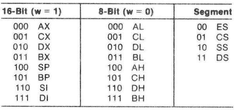
For more details, see my article on 8086 register codes.
Unexpected REP prefix
REP IMUL / IDIV
The REP prefix is used with string operations to cause the operation to be repeated across a block of memory.
However, if you use this prefix with an IMUL or IDIV instruction, it has the unexpected behavior
of negating the product or the quotient (source).
The reason for this behavior is that the string operations use an internal flag called F1 to indicate that a REP
prefix has been applied.
The multiply and divide code reuses this flag to track the sign of the input values, toggling F1 for each negative value.
If F1 is set, the value at the end is negated. (This handles "two negatives make a positive.")
The consequence is that the REP prefix puts the flag in the 1 state when the multiply/divide starts, so the computed sign
will be wrong at the end and the result is the negative of the expected result.
The microcode is fairly complex, so I won't show it here; I explain it in detail in this blog post.
REP RET
Wikipedia lists
REP RET (i.e. RET with a REP prefix) as a way to implement a two-byte return instruction.
This is kind of trivial; the RET microcode (like almost every instruction) doesn't use the F1 internal flag,
so the REP prefix has no effect.
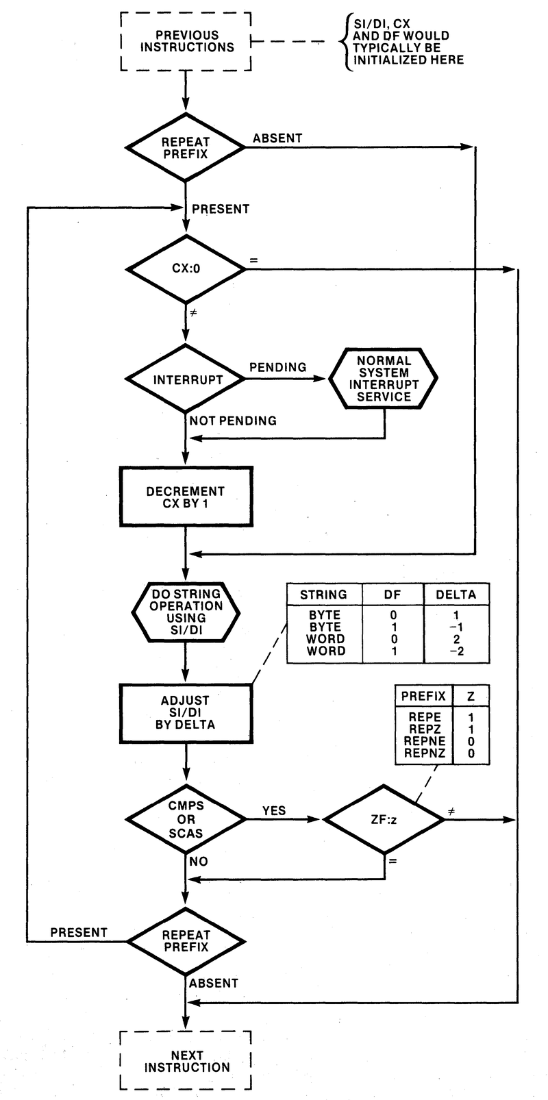
REPNZ MOVS/STOS
Wikipedia mentions that
the use of the REPNZ prefix (as opposed to REPZ) is undefined with string operations other than CMPS/SCAS.
An internal flag called F1Z distinguishes between the REPZ and REPNZ prefixes.
This flag is only used by CMPS/SCAS. Since the other string instructions ignore this flag, they will ignore the
difference between REPZ and REPNZ.
I wrote about string operations in more detail in this post.
Using a register instead of memory.
Some instructions are documented as requiring a memory operand. However, the ModR/M byte can specify a register. The behavior in these cases can be highly unusual, providing access to hidden registers. Examining the microcode shows how this happens.
LEA reg
Many instructions have a ModR/M byte that indicates the memory address that the instruction should use, perhaps through
a complicated addressing mode.
The LEA (Load Effective Address) instruction is different: it doesn't access the memory location but returns the address itself.
The undocumented part is that the ModR/M byte can specify a register instead of a memory location. In that case,
what does the LEA instruction do? Obviously it can't return the address of a register, but it needs to return something.
The behavior of LEA is explained by how the 8086 handles the ModR/M byte.
Before running the microcode corresponding to the instruction, the microcode engine calls a short micro-subroutine
for the particular addressing mode.
This micro-subroutine puts the desired memory address (the effective address) into the tmpA register.
The effective address is copied to the IND (Indirect) register and the value is loaded from memory if needed.
On the other hand, if the ModR/M byte specified a register instead of memory, no micro-subroutine is called.
(I explain ModR/M handling in more detail in this article.)
The microcode for LEA itself is just one line. It stores the effective address in the IND register into the specified destination register, indicated by N.
This assumes that the appropriate ModR/M micro-subroutine was called before this code, putting the effective address into IND.
IND → N RNI LEA: store IND register in destination, done
But if a register was specified instead of a memory location, no ModR/M micro-subroutine gets called.
Instead, the LEA instruction will return whatever value was left
in IND from before, typically the previous memory location that was accessed.
Thus, LEA can be used to read the value of the IND register, which is normally hidden from the programmer.
LDS reg, LES reg
The LDS and LES instructions load a far pointer from memory into the specified segment register and general-purpose register.
The microcode below assumes that the appropriate ModR/M micro-subroutine has set up IND and read the first value into OPR.
The microcode updates the destination register, increments IND by 2, reads the next value, and updates DS.
(The microcode for LES is a copy of this, but updates ES.)
OPR → N               LDS: Copy OPR to dest register
IND → tmpC  INC2 tmpC Set up incrementing IND by 2
Σ → IND     R DS,P0   Update IND, read next location
OPR → DS    RNI       Update DS
If the LDS instruction specifies a register instead of memory, a micro-subroutine will not be called, so IND and OPR
will have values from a previous instruction.
OPR will be stored in the destination register, while the DS value will be read from the address IND+2.
Thus, these instructions provide a mechanism to access the hidden OPR register.
JMP FAR rm
The JMP FAR rm instruction normally jumps to the far address stored in memory at the location indicated by the ModR/M byte.
(That is, the ModR/M byte indicates where the new PC and CS values are stored.)
But, as with LEA, the behavior is undocumented if the ModR/M byte specifies a register, since a register doesn't hold
a four-byte value.
The microcode explains what happens.
As with LEA, the code expects a micro-subroutine to put the address into the IND register.
In this case, the micro-subroutine also loads the value at that address (i.e. the destination PC) into tmpB.
The microcode increments IND by 2 to point to the CS word in memory and reads that into CS.
Meanwhile, it updates the PC with tmpB.
It suspends prefetching and flushes the queue, so instruction fetching will restart at the new address.
IND → tmpC  INC2 tmpC   JMP FAR rm: set up to add 2 to IND
Σ → IND     SUSP        Update IND, suspend prefetching
tmpB → PC   R DS,P0     Update PC with tmpB. Read new CS from specified address
OPR → CS    FLUSH RNI   Update CS, flush queue, done
If you specify a register instead of memory, the micro-subroutine won't get called.
Instead, the program counter will be loaded with whatever value was in tmpB and the CS segment register will
be loaded from the memory location two bytes after the location that IND was referencing.
Thus, this undocumented use of the instruction gives access to the otherwise-hidden tmpB register.
The end of undocumented instructions
Microprocessor manufacturers soon realized that undocumented instructions were a problem, since programmers find them and often use them. This creates an issue for future processors, or even revisions of the current processor: if you eliminate an undocumented instruction, previously-working code that used the instruction will break, and it will seem like the new processor is faulty.
The solution was for processors to detect undocumented instructions and prevent them from executing. By the early 1980s, processors had enough transistors (thanks to Moore's law) that they could include the circuitry to block unsupported instructions. In particular, the 80186/80188 and the 80286 generated a trap of type 6 when an unused opcode was executed, blocking use of the instruction.9 This trap is also known as #UD (Undefined instruction trap).10
Conclusions
The 8086, like many early microprocessors, has undocumented instructions but no traps to stop them from executing.11
For the 8086, these fall into several categories.
Many undocumented instructions simply mirror existing instructions.
Some instructions are implemented but not documented for one reason or another, such as SALC and POP CS.
Other instructions can be used outside their normal range, such as AAM and AAD.
Some instructions are intended to work only with a memory address, so specifying a register can have
strange effects such as revealing the values of the hidden IND and OPR registers.
Keep in mind that my analysis is based on transistor-level simulation and examining the microcode; I haven't verified the behavior on a physical 8086 processor. Please let me know if you see any errors in my analysis or undocumented instructions that I have overlooked. Also note that the behavior could change between different versions of the 8086; in particular, some versions by different manufacturers (such as the NEC V20 and V30) are known to be different.
I plan to write more about the 8086, so follow me on Twitter @kenshirriff or RSS for updates. I've also started experimenting with Mastodon recently as @kenshirriff@oldbytes.space and Bluesky as @righto.com so you can follow me there too.
Notes and references
-
The 6502 processor, for instance, has illegal instructions with various effects, including causing the processor to hang. The article How MOS 6502 illegal opcodes really work describes in detail how the instruction decoding results in various illegal opcodes. Some of these opcodes put the internal bus into a floating state, so the behavior is electrically unpredictable. ↩
-
The 8086 used up almost all the single-byte opcodes, which made it difficult to extend the instruction set. Most of the new instructions for the 386 or later are multi-byte opcodes, either using
0Fas a prefix or reusing the earlier REP prefix (F3). Thus, the x86 instruction set is less efficient than it could be, since many single-byte opcodes were "wasted" on hardly-used instructions such as BCD arithmetic, forcing newer instructions to be multi-byte. ↩ -
For details on the "magic instruction" hidden in the 8086 microcode, see NEC v. Intel: Will Hardware Be Drawn into the Black Hole of Copyright Editors page 49. I haven't found anything stating that
SALCwas the hidden instruction, but this is the only undocumented instruction that makes sense as something deliberately put into the microcode. The court case is complicated since NEC had a licensing agreement with Intel, so I'm skipping lots of details. See NEC v. Intel: Breaking new ground in the law of copyright for more. ↩ -
The microcode listings are based on Andrew Jenner's disassembly. I have made some modifications to (hopefully) make it easier to understand. ↩
-
Specifying the instruction through the ModR/M reg field may seem a bit random, but there's a reason for this. A typical instruction such as
ADDhas two arguments specified by the ModR/M byte. But other instructions such as shift instructions orNOTonly take one argument. For these instructions, the ModR/Mregfield would be wasted if it specified a register. Thus, using theregfield to specify instructions that only use one argument makes the instruction set more efficient. ↩ -
Note that "normal" ALU operations are specified by bits 5-3 of the instruction; in order these are
ADD,OR,ADC,SBB,AND,SUB,XOR, andCMP. These are exactly the same ALU operations that the "Immed" group performs, specified by bits 5-3 of the second byte. This illustrates how the same operation selection mechanism (theXregister) is used in both cases. Bit 6 of the instruction switches between the set of arithmetic/logic instructions and the set of shift/rotate instructions. ↩ -
As far as I can tell, SETMO isn't used by the microcode. Thus, I think that SETMO wasn't deliberately implemented in the ALU, but is a consequence of how the ALU's control logic is implemented. That is, all the even entries are left shifts and the odd entries are right shifts, so operation 6 activates the left-shift circuitry. But it doesn't match a specific left shift operation, so the ALU doesn't get configured for a "real" left shift. In other words, the behavior of this instruction is due to how the ALU handles a case that it wasn't specifically designed to handle.
This function is implemented in the ALU somewhat similar to a shift left. However, instead of passing each input bit to the left, the bit from the right is passed to the left. That is, the input to bit 0 is shifted left to all of the bits of the result. By setting this bit to 1, all bits of the result are set, yielding the minus 1 result. ↩
-
This footnote provides some references for the "Immed" opcodes. The 8086 datasheet has an opcode map showing opcodes
80through83as valid. However, in the listings of individual instructions it only shows80and81for logical instructions (i.e. bit 1 must be 0), while it shows80-83for arithmetic instructions. The modern Intel 64 and IA-32 Architectures Software Developer's Manual is also contradictory. Looking at the instruction reference forAND(Vol2A3-78), for instance, shows opcodes80,81, and83, explicitly labeling83as sign-extended. But the opcode map (Table A-2 Vol2DA-7) shows80-83as defined except for82in64-bit mode. The instruction bit diagram (Table B-13Vol2DB-7) shows80-83valid for the arithmetic and logical instructions. ↩ -
The 80286 was more thorough about detecting undefined opcodes than the 80186, even taking into account the differences in instruction set. The 80186 generates a trap when
0F,63-67,F1, orFFFFis executed. The 80286 generates invalid opcode exception number 6 (#UD) on any undefined opcode, handling the following cases:- The first byte of an instruction is completely invalid (e.g., 64H).
- The first byte indicates a 2-byte opcode and the second byte is invalid (e.g., 0F followed by 0FFH).
- An invalid register is used with an otherwise valid opcode (e.g., MOV CS,AX).
- An invalid opcode extension is given in the REG field of the ModR/M byte (e.g., 0F6H /1).
- A register operand is given in an instruction that requires a memory operand (e.g., LGDT AX).
-
In modern x86 processors, most undocumented instructions cause faults. However, there are still a few undocumented instructions that don't fault. These may be for internal use or corner cases of documented instructions. For details, see Breaking the x86 Instruction Set, a video from Black Hat 2017. ↩
-
Several sources have discussed undocumented 8086 opcodes before. The article Undocumented 8086 Opcodes describes undocumented opcodes in detail. Wikipedia has a list of undocumented x86 instructions. The book Undocumented PC discusses undocumented instructions in the 8086 and later processors. This StackExchange Retrocomputing post describes undocumented instructions. These Hacker News comments discuss some undocumented instructions. There are other sources with more myth than fact, claiming that the 8086 treats undocumented instructions as NOPs, for instance. ↩
Subject: Reverse-engineering the 8086 processor's address and data pin circuits
The Intel 8086 microprocessor (1978) started the x86 architecture that continues to this day. In this blog post, I'm focusing on a small part of the chip: the address and data pins that connect the chip to external memory and I/O devices. In many processors, this circuitry is straightforward, but it is complicated in the 8086 for two reasons. First, Intel decided to package the 8086 as a 40-pin DIP, which didn't provide enough pins for all the functionality. Instead, the 8086 multiplexes address, data, and status. In other words, a pin can have multiple roles, providing an address bit at one time and a data bit at another time.
The second complication is that the 8086 has a 20-bit address space (due to its infamous segment registers), while the data bus is 16 bits wide. As will be seen, the "extra" four address bits have more impact than you might expect. To summarize, 16 pins, called AD0-AD15, provide 16 bits of address and data. The four remaining address pins (A16-A19) are multiplexed for use as status pins, providing information about what the processor is doing for use by other parts of the system. You might expect that the 8086 would thus have two types of pin circuits, but it turns out that there are four distinct circuits, which I will discuss below.
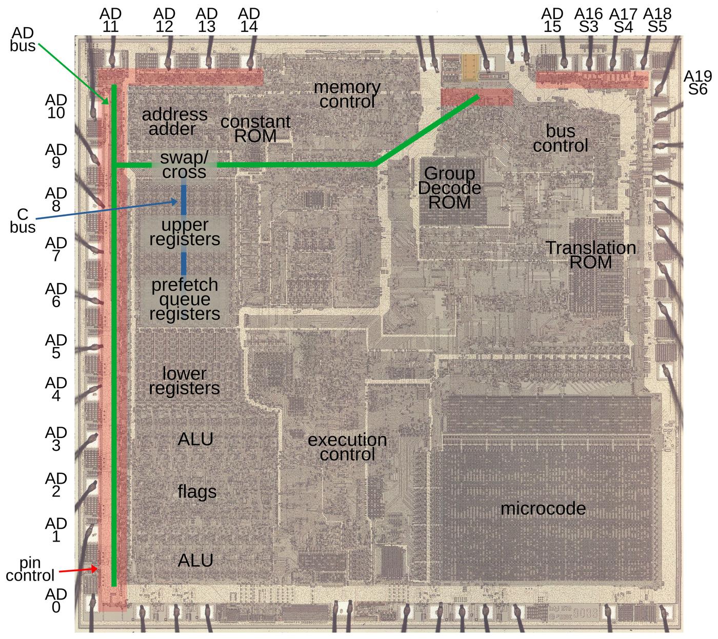
The microscope image above shows the silicon die of the 8086. In this image, the metal layer on top of the chip is visible, while the silicon and polysilicon underneath are obscured. The square pads around the edge of the die are connected by tiny bond wires to the chip's 40 external pins. The 20 address pins are labeled: Pins AD0 through AD15 function as address and data pins. Pins A16 through A19 function as address pins and status pins.1 The circuitry that controls the pins is highlighted in red. Two internal busses are important for this discussion: the 20-bit AD bus (green) connects the AD pins to the rest of the CPU, while the 16-bit C bus (blue) communicates with the registers. These buses are connected through a circuit that can swap the byte order or shift the value. (The lines on the diagram are simplified; the real wiring twists and turns to fit the layout. Moreover, the C bus (blue) has its bits spread across the width of the register file.)
Segment addressing in the 8086
One goal of the 8086 design was to maintain backward compatibility with the earlier 8080 processor.2 This had a major impact on the 8086's memory design, resulting in the much-hated segment registers. The 8080 (like most of the 8-bit processors of the early 1970s) had a 16-bit address space, able to access 64K (65,536 bytes) of memory, which was plenty at the time. But due to the exponential growth in memory capacity described by Moore's Law, it was clear that the 8086 needed to support much more. Intel decided on a 1-megabyte address space, requiring 20 address bits. But Intel wanted to keep the 16-bit memory addresses used by the 8080.
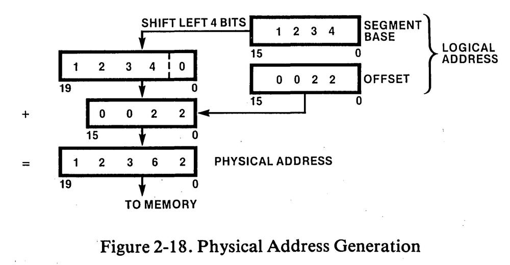
The solution was to break memory into segments. Each segment was 64K long, so a 16-bit offset was sufficient to access memory in a segment. The segments were allocated in a 1-megabyte address space, with the result that you could access a megabyte of memory, but only in 64K chunks.3 Segment addresses were also 16 bits, but were shifted left by 4 bits (multiplied by 16) to support the 20-bit address space.
Thus, every memory access in the 8086 required a computation of the physical address. The diagram below illustrates this process: the logical address consists of the segment base address and the offset within the segment. The 16-bit segment register was shifted 4 bits and added to the 16-bit offset to yield the 20-bit physical memory address.
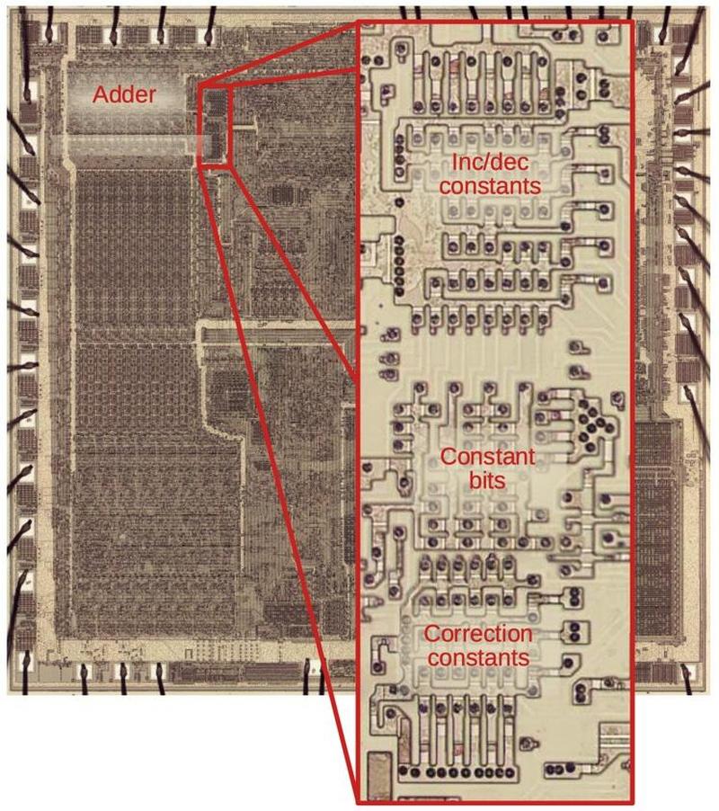
This address computation was not performed by the regular ALU (Arithmetic/Logic Unit), but by a separate adder that was devoted to address computation. The address adder is visible in the upper-left corner of the die photo. I will discuss the address adder in more detail below.
The AD bus and the C Bus
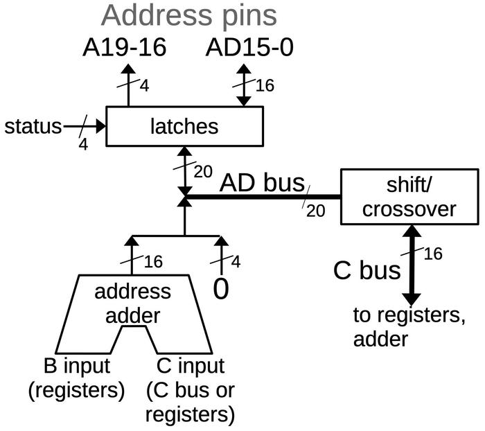
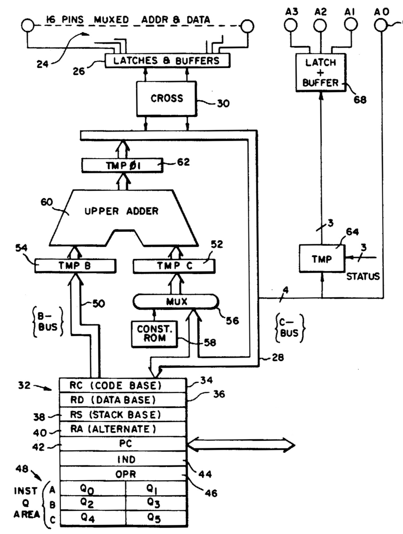
The 8086 has multiple internal buses to move bits internally, but the relevant ones are the AD bus and the C bus. The AD bus is a 20-bit bus that connects the 20 address/data pins to the internal circuitry.4 A 16-bit bus called the C bus provides the connection between the AD bus, the address adder and some of the registers.5 The diagram below shows the connections. The AD bus can be connected to the 20 address pins through latches. The low 16 pins can also be used for data input, while the upper 4 pins can also be used for status output. The address adder performs the 16-bit addition necessary for segment arithmetic. Its output is shifted left by four bits (i.e. it has four 0 bits appended), producing the 20-bit result. The inputs to the adder are provided by registers, a constant ROM that holds small constants such as +1 or -2, or the C bus.
The shift/crossover circuit provides the interface between these two buses, handling the 20-bit to 16-bit conversion. The busses can be connected in three ways: direct, crossover, or shifted.6 The direct mode connects the 16 bits of the C bus to the lower 16 bits of the address/data pins. This is the standard mode for transferring data between the 8086's internal circuitry and the data pins. The crossover mode performs the same connection but swaps the bytes. This is typically used for unaligned memory accesses, where the low memory byte corresponds to the high register byte, or vice versa. The shifted mode shifts the 20-bit AD bus value four positions to the right. In this mode, the 16-bit output from the address adder goes to the 16-bit C bus. (The shift is necessary to counteract the 4-bit shift applied to the address adder's output.) Control circuitry selects the right operation for the shift/crossover circuit at the right time.7
Two of the registers are invisible to the programmer but play an important role in memory accesses.
The IND (Indirect) register specifies the memory address; it holds the 16-bit memory offset in a segment.
The OPR (Operand) register holds the data value.9
The IND and OPR registers are not accessed directly by the programmer; the microcode for a machine instruction moves the appropriate
values to these registers prior to the write.
Overview of a write cycle
I hesitate to present a timing diagram, since I may scare off of my readers, but the 8086's communication is designed around a four-step bus cycle. The diagram below shows simplified timing for a write cycle, when the 8086 writes to memory or an I/O device.8 The external bus activity is organized as four states, each one clock cycle long: T1, T2, T3, T4. These T states are very important since they control what happens on the bus. During T1, the 8086 outputs the address on the pins. During the T2, T3, and T4 states, the 8086 outputs the data word on the pins. The important part for this discussion is that the pins are multiplexed depending on the T-state: the pins provide the address during T1 and data during T2 through T4.
There two undocumented T states that are important to the bus cycle. The physical address is computed in the two clock cycles before T1 so the address will be available in T1. I give these "invisible" T states the names TS (start) and T0.
The address adder
The operation of the address adder is a bit tricky since the 16-bit adder must generate a 20-bit physical address. The adder has two 16-bit inputs: the B input is connected to the upper registers via the B bus, while the C input is connected to the C bus. The segment register value is transferred over the B bus to the adder during the second half of the TS state (that is, two clock cycles before the bus cycle becomes externally visible during T1). Meanwhile, the address offset is transferred over the C bus to the adder, but the adder's C input shifts the value four bits to the right, discarding the four low bits. (As will be explained later, the pin driver circuits latch these bits.) The adder's output is shifted left four bits and transferred to the AD bus during the second half of T0. This produces the upper 16 bits of the 20-bit physical memory address. This value is latched into the address output flip-flops at the start of T1, putting the computed address on the pins. To summarize, the 20-bit address is generated by storing the 4 low-order bits during T0 and then the 16 high-order sum bits during T1.
The address adder is not needed for segment arithmetic during T1 and T2.
To improve performance, the 8086 uses the adder during this idle time to increment or decrement memory addresses.
For instance, after popping a word from the stack, the stack pointer needs to be incremented by 2.
The address adder can do this increment "for free" during T1 and T2, leaving the ALU available for other operations.10
Specifically, the adder updates the memory address in IND, incrementing it or decrementing it as appropriate.
First, the IND value is transferred over the B bus to the adder during the second half of T1.
Meanwhile, a constant (-3 to +2) is loaded from the Constant ROM and transferred to the adder's C input.
The output from the adder is transferred to the AD bus during the second half of T2.
As before, the output is shifted four bits to the left. However, the shift/crossover circuit between the AD bus and the C bus
is configured to shift four bits to the right, canceling the adder's shift.
The result is that the C bus gets the 16-bit sum from the adder, and this value is stored in the IND register.11
For more information on the implemenation of the address adder, see my previous blog post.
The pin driver circuit
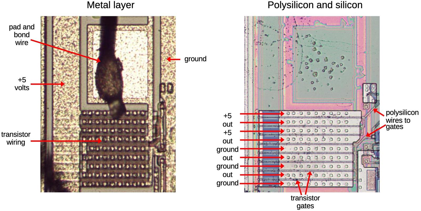
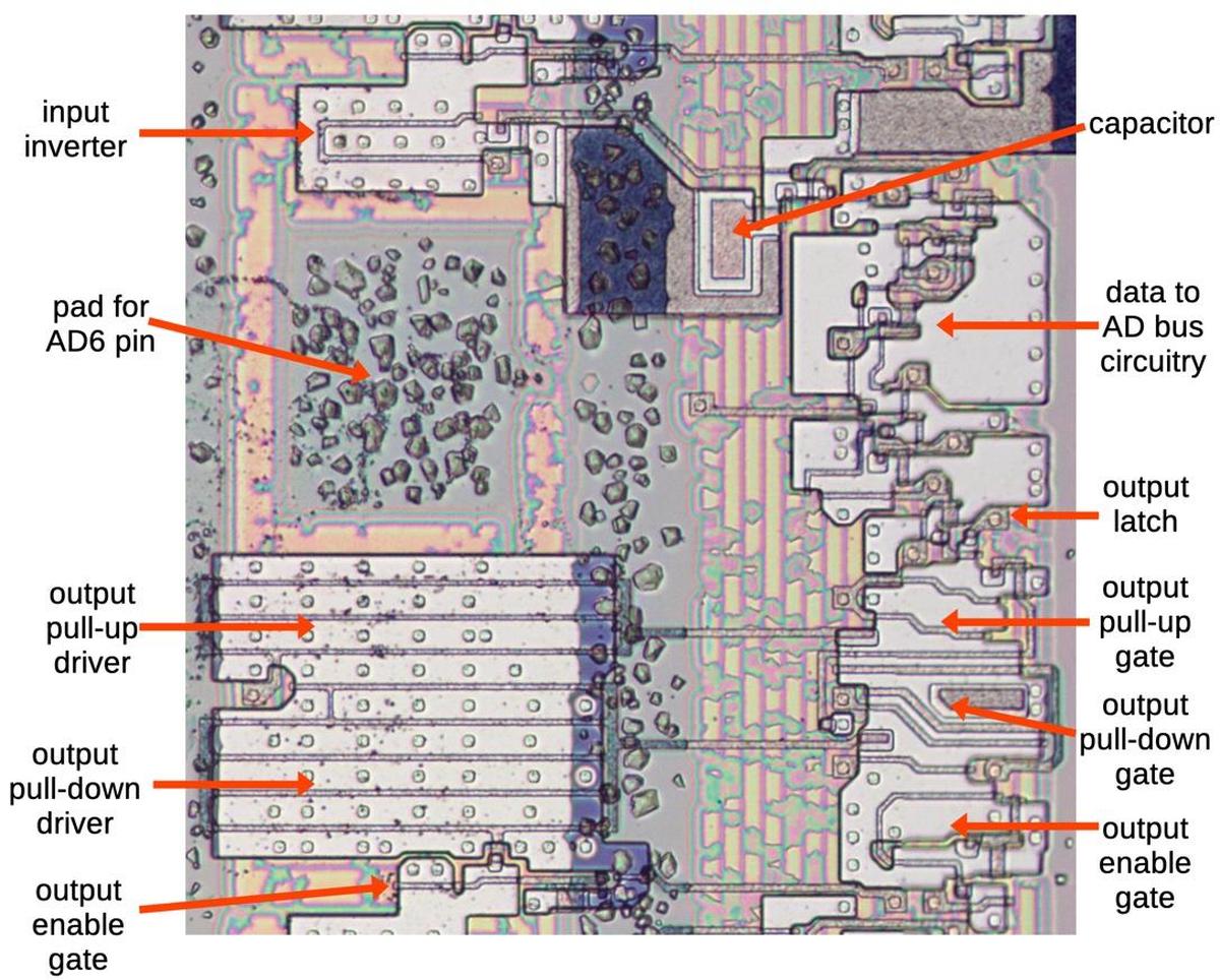
Now I'll dive down to the hardware implementation of an output pin. When the 8086 chip communicates with the outside world, it needs to provide relatively high currents. The tiny logic transistors can't provide enough current, so the chip needs to use large output transistors. To fit the large output transistors on the die, they are constructed of multiple wide transistors in parallel.12 Moreover, the drivers use a somewhat unusual "superbuffer" circuit with two transistors: one to pull the output high, and one to pull the output low.13
The diagram below shows the transistor structure for one of the output pins (AD10), consisting of three parallel transistors between the output and +5V, and five parallel transistors between the output and ground. The die photo on the left shows the metal layer on top of the die. This shows the power and ground wiring and the connections to the transistors. The photo on the right shows the die with the metal layer removed, showing the underlying silicon and the polysilicon wiring on top. A transistor gate is formed where a polysilicon wire crosses the doped silicon region. Combined, the +5V transistors are equivalent to about 60 typical transistors, while the ground transistors are equivalent to about 100 typical transistors. Thus, these transistors provide substantially more current to the output pin.
Tri-state output driver
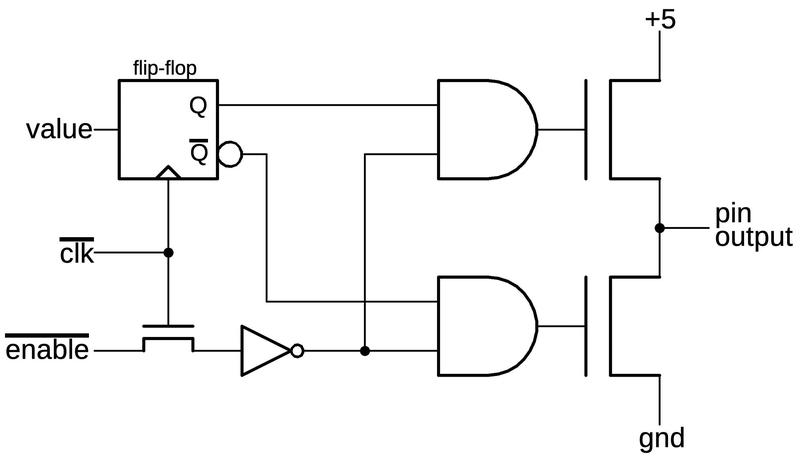
The output circuit for an address pin uses a tri-state buffer, which allows the output to be disabled by putting it into a high-impedance "tri-state" configuration. In this state, the output is not pulled high or low but is left floating. This capability allows the pin to be used for data input. It also allows external devices to device can take control of the bus, for instance, to perform DMA (direct memory access).
The pin is driven by two large MOSFETs, one to pull the output high and one to pull it low. (As described earlier, each large MOSFET is physically multiple transistors in parallel, but I'll ignore that for now.) If both MOSFETs are off, the output floats, neither on nor off.
The tri-state output is implemented by driving the MOSFETs with two "superbuffer"15 AND gates.
If the enable input is low, both AND gates produce a low output and both output transistors are off.
On the other hand, if enable is high, one AND gate will be on and one will be off.
The desired output value is loaded into a flip-flop to hold it,14
and the flip-flop turns one of the output transistors on, driving the output pin high or low as appropriate.
(Conveniently, the flip-flop provides the data output Q and the inverted data output Q.)
Generally, the address pin outputs are enabled for T1-T4 of a write but only during T1 for a read.16
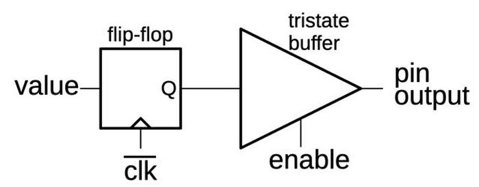
In the remainder of the discussion, I'll use the tri-state buffer symbol below, rather than showing the implementation of the buffer.
AD4-AD15
Pins AD4-AD15 are "typical" pins, avoiding the special behavior of the top and bottom pins, so I'll discuss them first.
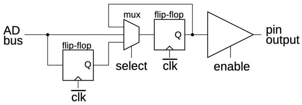
The behavior of these pins is that the value on the AD bus is latched by the circuit and then put on the output pin
under the control of the enaable signal.
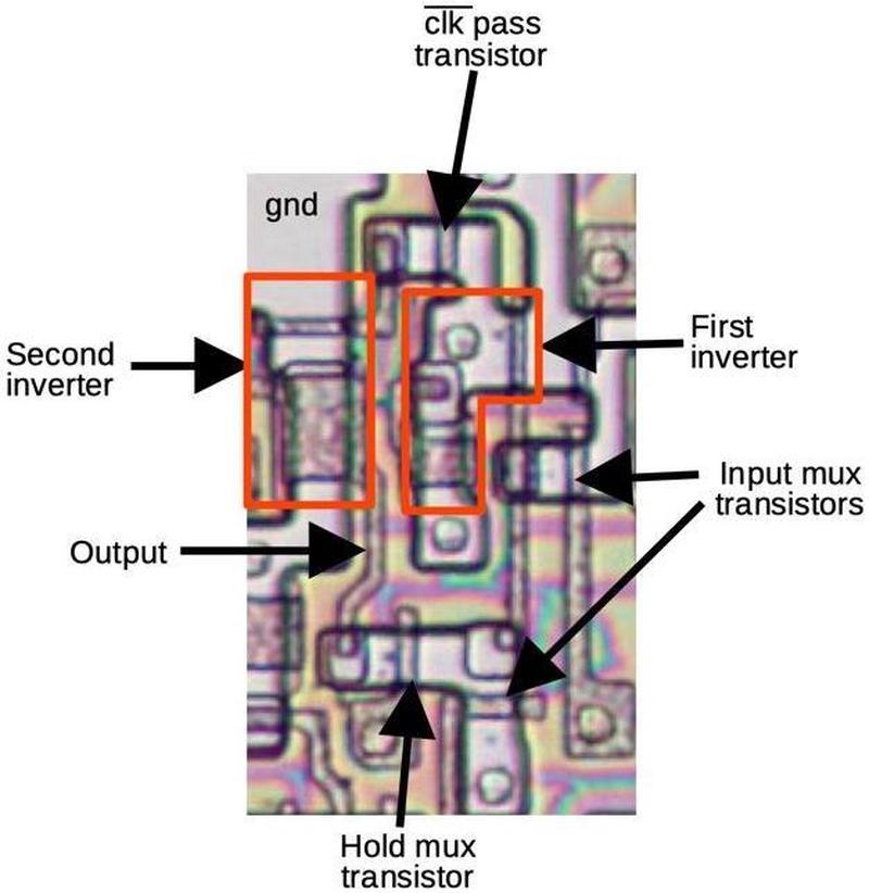
The circuit has three parts: a multiplexer to select the output value, a flip-flop to hold the output value, and a tri-state driver to
provide the high-current output to the pin.
In more detail, the multiplexer selects either the value on the AD bus or the current output from the flip-flop.
That is, the multiplexer can either load a new value into the flip-flop or hold the existing value.17
The flip-flop latches the input value on the falling edge of the clock, passing it to the output driver.
If the enable line is high, the output driver puts this value on the corresponding address pin.
For a write, the circuit latches the address value on the bus during the second half of T0 and puts it on the pins during T1.
During the second half of the T1 state, the data word is transferred from the OPR register over the C bus to the AD bus and loaded
into the AD pin latches.
The word is transferred from the latches to the pins during T2 and held for the remainder of the bus cycle.
AD0-AD3
The four low address bits have a more complex circuit because these address bits are latched from the bus before the address adder computes its sum, as described earlier. The memory offset (before the segment addition) will be on the C bus during the second half of TS and is loaded into the lower flip-flop. This flip-flop delays these bits for one clock cycle and then they are loaded into the upper flip-flop. Thus, these four pins pick up the offset prior to the addition, while the other pins get the result of the segment addition.
For data, the AD0-AD3 pins transfer data directly from the AD bus to the pin latch, bypassing the delay that was used to get the address bits. That is, the AD0-AD3 pins have two paths: the delayed path used for addresses during T0 and the direct path otherwise used for data. Thus, the multiplexer has three inputs: two for these two paths and a third loop-back input to hold the flip-flop value.
A16-A19: status outputs
The top four pins (A16-A19) are treated specially, since they are not used for data. Instead, they provide processor status during T2-T4.18 The pin latches for these pins are loaded with the address during T0 like the other pins, but loaded with status instead of data during T1. The multiplexer at the input to the latch selects the address bit during T0 and the status bit during T1, and holds the value otherwise. The schematic below shows how this is implemented for A16, A17, and A19.
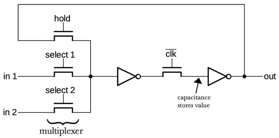
Address pin A18 is different because it indicates the current status of the interrupt enable flag bit. This status is updated every clock cycle, unlike the other pins. To implement this, the pin has a different circuit that isn't latched, so the status can be updated continuously. The clocked transistors act as "pass transistors", passing the signal through when active. When a pass transistor is turned off, the following logic gate holds the previous value due to the capacitance of the wiring. Thus, the pass transistors provide a way of holding the value through the clock cycle. The flip-flops are implemented with pass transistors internally, so in a sense the circuit below is a flip-flop that has been "exploded" to provide a second path for the interrupt status.
Reads
A memory or I/O read also uses a 4-state bus cycle, slightly different from the write cycle.
During T1, the address is provided on the pins, the same as for a write.
After that, however, the output circuits are tri-stated so they float, allowing the external memory to put data on the bus.
The read data on the pin is put on the AD bus at the start of the T4 state.
From there, the data passes through the crossover circuit to the C bus. Normally the 16 data bits pass straight through to
the C bus, but the bytes will be swapped if the memory access is unaligned.
From the C bus, the data is written to the OPR register, a byte or a word as appropriate.
(For an instruction prefetch, the word is written to a prefetch queue register instead.)
To support data input on the AD0-AD15 pins, they have a circuit to buffer the input data and transfer it to the AD bus. The incoming data bit is buffered by the two inverters and sampled when the clock is high. If the enable' signal is low, the data bit is transferred to the AD bus when the clock is low.19 The two MOSFETs act as a "superbuffer", providing enough current for the fairly long AD bus. I'm not sure what the capacitor accomplishes, maybe avoiding a race condition if the data pin changes just as the clock goes low.20
This circuit has a second role, precharging the AD bus high when the clock is low, if there's no data. Precharging a bus is fairly common in the 8086 (and other NMOS processors) because NMOS transistors are better at pulling a line low than pulling it high. Thus, it's often faster to precharge a line high before it's needed and then pull it low for a 0.21
Since pins A16-A19 are not used for data, they operate the same for reads as for writes: providing address bits and then status.
The pin circuit on the die
The diagram below shows how the pin circuitry appears on the die. The metal wiring has been removed to show the silicon and polysilicon. The top half of the image is the input circuitry, reading a data bit from the pin and feeding it to the AD bus. The lower half of the image is the output circuitry, reading an address or data bit from the AD bus and amplifying it for output via the pad. The light gray regions are doped, conductive silicon. The thin tan lines are polysilicon, which forms transistor gates where it crosses doped silicon.
A historical look at pins and timing
The number of pins on Intel chips has grown exponentially, more than a factor of 100 in 50 years. In the early days, Intel management was convinced that a 16-pin package was large enough for any integrated circuit. As a result, the Intel 4004 processor (1971) was crammed into a 16-pin package. Intel chip designer Federico Faggin22 describes 16-pin packages as a completely silly requirement that was throwing away performance, but the "God-given 16 pins" was like a religion at Intel. When Intel was forced to use 18 pins by the 1103 memory chip, it "was like the sky had dropped from heaven" and he had "never seen so many long faces at Intel." Although the 8008 processor (1972) was able to use 18 pins, this low pin count still harmed performance by forcing pins to be used for multiple purposes.
The Intel 8080 (1974) had a larger, 40-pin package that allowed it to have 16 address pins and 8 data pins. Intel stuck with this size for the 8086, even though competitors used larger packages with more pins.23 As processors became more complex, the 40-pin package became infeasible and the pin count rapidly expanded; The 80286 processor (1982) had a 68-pin package, while the i386 (1985) had 132 pins; the i386 needed many more pins because it had a 32-bit data bus and a 24- or 32-bit address bus. The i486 (1989) went to 196 pins while the original Pentium had 273 pins. Nowadays, a modern Core I9 processor uses the FCLGA1700 socket with a whopping 1700 contacts.
Looking at the history of Intel's bus timing, the 8086's complicated memory timing goes back to the Intel 8008 processor (1972). Instruction execution in the 8008 went through a specific sequence of timing states; each clock cycle was assigned a particular state number. Memory accesses took three cycles: the address was sent to memory during states T1 and T2, half of the address at a time since there were only 8 address pins. During state T3, a data byte was either transmitted to memory or read from memory. Instruction execution took place during T4 and T5. State signals from the 8008 chip indicated which state it was in.
The 8080 used an even more complicated timing system. An instruction consisted of one to five "machine cycles", numbered M1 through M5, where each machine cycle corresponded to a memory or I/O access. Each machine cycle consisted of three to five states, T1 through T5, similar to the 8008 states. The 8080 had 10 different types of machine cycle such as instruction fetch, memory read, memory write, stack read or write, or I/O read or write. The status bits indicated the type of machine cycle. The 8086 kept the T1 through T4 memory cycle. Because the 8086 decoupled instruction prefetching from execution, it no longer had explicit M machine cycles. Instead, it used status bits to indicate 8 types of bus activity such as instruction fetch, read data, or write I/O.
Conclusions
Well, address pins is another subject that I thought would be straightforward to explain but turned out to be surprisingly complicated. Many of the 8086's design decisions combine in the address pins: segmented addressing, backward compatibility, and the small 40-pin package. Moreover, because memory accesses are critical to performance, Intel put a lot of effort into this circuitry. Thus, the pin circuitry is tuned for particular purposes, especially pin A18 which is different from all the rest.
There is a lot more to say about memory accesses and how the 8086's Bus Interface Unit performs them. The process is very complicated, with interacting state machines for memory operation and instruction prefetches, as well as handling unaligned memory accesses. I plan to write more, so follow me on Twitter @kenshirriff or RSS for updates. I've also started experimenting with Mastodon recently as @kenshirriff@oldbytes.space and Bluesky as @righto.com so you can follow me there too.
Notes and references
-
In the discussion, I'll often call all the address pins "AD" pins for simplicity, even though pins 16-19 are not used for data. ↩
-
The 8086's compatibility with the 8080 was somewhat limited since the 8086 had a different instruction set. However, Intel provided a conversion program called CONV86 that could convert 8080/8085 assembly code into 8086 assembly code that would usually work after minor editing. The 8086 was designed to make this process straightforward, with a mapping from the 8080's registers onto the 8086's registers, along with a mostly-compatible instruction set. (There were a few 8080 instructions that would be expanded into multiple 8086 instructions.) The conversion worked for straightforward code, but didn't work well with tricky, self-modifying code, for instance. ↩
-
To support the 8086's segment architecture, programmers needed to deal with "near" and "far" pointers. A near pointer consisted of a 16-bit offset and could access 64K in a segment. A far pointer consisted of a 16-bit offset along with a 16-bit segment address. By modifying the segment register on each access, the full megabyte of memory could be accessed. The drawbacks were that far pointers were twice as big and were slower. ↩
-
The 8086 patent provides a detailed architectural diagram of the 8086. I've extracted part of the diagram below. In most cases the diagram is accurate, but its description of the C bus doesn't match the real chip. There are some curious differences between the patent diagram and the actual implementation of the 8086, suggesting that the data pins were reorganized between the patent and the completion of the 8086. The diagram shows the address adder (called the Upper Adder) connected to the C bus, which is connected to the address/data pins. In particular, the patent shows the data pins multiplexed with the high address pins, while the low address pins A3-A0 are multiplexed with three status signals. The actual implementation of the 8086 is the other way around, with the data pins multiplexed with the low address pins while the high address pins A19-A16 are multiplexed with the status signals. Moreover, the patent doesn't show anything corresponding to what I call the AD bus; I made up that name. The moral is that while patents can be very informative, they can also be misleading.
A diagram from patent US4449184 showing the connections to the address pins. This diagram does not match the actual chip. The diagram also shows the old segment register names: RC, RD, RS, and RA became CS, DS, SS, and ES. -
The C bus is connected to the PC, OPR, and IND registers, as well as the prefetch queue, but is not connected to the segment registers. Two other buses (the ALU bus and the B bus) provide access to the segment registers. ↩
-
Swapping the bytes on the data pins is required in a few cases. The 8086 has a 16-bit data bus, so transfers are usually a 16-bit word, copied directly between memory and a register. However, the 8086 also allows 8-bit operations, in which case either the top half or bottom half of the word is accessed. Loading an 8-bit value from the top half of a memory word into the bottom half of a register uses the crossover circuit. Another case is performing a 16-bit access to an "unaligned" address, that is, an odd address so the word crosses the normal word boundaries. From the programmer's perspective, an unaligned access is permitted (unlike many RISC processors), but the hardware converts this access into two 8-bit accesses, so the bus itself never handles an unaligned access.
The 8086 has the ability to access a single memory byte out of a word, either for a byte operation or for an unaligned word operation. This behavior has some important consequences on the address pins. In particular, the low address pin AD0 doesn't behave like the rest of the address pins due to the special handling of odd addresses. Instead, this pin indicates which half of the word to transfer. The AD0 line is low (0) when the lower portion of the bus transfers a byte. Another pin, BHE (Bus High Enable) has a similar role for the upper half of the bus: it is low (0) if a byte is transferred over D15-D8. (Keep in mind that the 8086 is little-endian, so the low byte of the word is first in memory, at the even address.)
The following table summarizes how BHE and A0 work together to select a byte or word. When accessing a byte at an odd address, A0 is odd as you might expect.
↩Access type BHE A0 Word 0 0 Low byte 1 0 High byte 0 1 -
The
cbus-adbus-shiftsignal is activated duringT2, when a memory index is being updated, either the instruction pointer or theINDregister. The address adder is used to update the register and the shift undoes the 4-bit left shift applied to the adder's output. The shift is also used for theCORRmicro-instruction, which corrects the instruction pointer to account for prefetching. TheCORRmicro-instruction generates a "fake" short bus cycle in which the constant ROM and the address adder are used during T0. I discuss theCORRmicro-instruction in more detail in this post. ↩ -
I've made the timing diagram somewhat idealized so actions line up with the clock. In the real datasheet, all the signals are skewed by various amounts so the timing is more complicated. Moreover, if the memory device is slow, it can insert "wait" states between T3 and T4. (Cheap memory was slower and would need wait states.) Moreover, actions don't exactly line up with the clock. I'm also omitting various control signals. The datasheet has pages of timing constraints on exactly when signals can change. ↩
-
Instruction prefetches don't use the
INDandOPRregisters. Instead, the address is specified by the Instruction Pointer (or Program Counter), and the data is stored directly into one of the instruction prefetch registers. ↩ -
A single memory operation takes six clock cycles: two preparatory cycles to compute the address before the four visible cycles. However, if multiple memory operations are performed, the operations are overlapped to achieve a degree of pipelining. Specifically, the address calculation for the next memory operation takes place during the last two clock cycles of the current memory operation, saving two clock cycles. That is, for consecutive bus cycles, T3 and T4 overlap with TS and T0 of the next cycle. In other words, during T3 and T4 of one bus cycle, the memory address gets computed for the next bus cycle. This pipelining improves performance, compared to taking 6 clock cycles for each bus cycle. ↩
-
The
POPoperation is an example of how the address adder updates a memory pointer. In this case, the stack address is moved from the Stack Pointer to theINDregister in order to perform the memory read. As part of the read operation, theINDregister is incremented by 2. The address is then moved from theINDregister to the Stack Pointer. Thus, the address adder not only performs the segment arithmetic, but also computes the new value for theSPregister.Note that the increment/decrement of the
INDregister happens after the memory operation. For stack operations, the SP must be decremented before aPUSHand incremented after aPOP. The adder cannot perform a predecrement, so thePUSHinstruction uses the ALU (Arithmetic/Logic Unit) to perform the decrement. ↩ -
The current from an MOS transistor is proportional to the width of the gate divided by the length (the W/L ratio). Since the minimum gate width is set by the manufacturing process, increasing the width of the gate (and thus the overall size of the transistor) is how the transistor's current is increased. ↩
-
Using one transistor to pull the output high and one to pull the output low is normal for CMOS gates, but it is unusual for NMOS chips like the 8086. A normal NMOS gate only has active transistor to pull the output low and uses a depletion-mode transistor to provide a weak pull-up current, similar to a pull-up resistor. I discuss superbuffers in more detail here. ↩
-
The flip-flop is controlled by the inverted clock signal, so the output will change when the clock goes low. Meanwhile, the
enablesignal is dynamically latched by a MOSFET, also controlled by the inverted clock. (When the clock goes high, the previous value will be retained by the gate capacitance of the inverter.) ↩ -
The superbuffer AND gates are constructed on the same principle as the regular superbuffer, except with two inputs. Two transistors in series pull the output high if both inputs are high. Two transistors in parallel pull the output low if either input is low. The low-side transistors are driven by inverted signals. I haven't drawn these signals on the schematic to simplify it.
The superbuffer AND gates use large transistors, but not as large as the output transistors, providing an intermediate amplification stage between the small internal signals and the large external signals. Because of the high capacitance of the large output transistors, they need to be driven with larger signals. There's a lot of theory behind how transistor sizes should be scaled for maximum performance, described in the book Logical Effort. Roughly speaking, for best performance when scaling up a signal, each stage should be about 3 to 4 times as large as the previous one, so a fairly large number of stages are used (page 21). The 8086 simplifies this with two stages, presumably giving up a bit of performance in exchange for keeping the drivers smaller and simpler. ↩
-
The enable circuitry has some complications. For instance, I think the address pins will be enabled if a cycle was going to be T1 for a prefetch but then got preempted by a memory operation. The bus control logic is fairly complicated. ↩
-
The multiplexer is implemented with pass transistors, rather than gates. One of the pass transistors is turned on to pass that value through to the multiplexer's output. The flip-flop is implemented with two pass transistors and two inverters in alternating order. The first pass transistor is activated by the clock and the second by the complemented clock. When a pass transistor is off, its output is held by the gate capacitance of the inverter, somewhat like dynamic RAM. This is one reason that the 8086 has a minimum clock speed: if the clock is too slow, these capacitively-held values will drain away. ↩
-
The status outputs on the address pins are defined as follows: A16/S3, A17/S4: these two status lines indicate which relocation register is being used for the memory access, i.e. the stack segment, code segment, data segment, or alternate segment. Theoretically, a system could use a different memory bank for each segment and increase the total memory capacity to 4 megabytes.
A18/S5: indicates the status of the interrupt enable bit. In order to provide the most up-to-date value, this pin has a different circuit. It is updated at the beginning of each clock cycle, so it can change during a bus cycle. The motivation for this is presumably so peripherals can determine immediately if the interrupt enable status changes.
A19/S6: the documentation calls this a status output, even though it always outputs a status of 0. ↩ -
For a read, the enable signal is activated at the end of T3 and the beginning of T4 to transfer the data value to the AD bus. The signal is gated by the READY pin, so the read doesn't happen until the external device is ready. The 8086 will insert Tw wait states in that case. ↩
-
The datasheet says that a data value must be held steady for 10 nanoseconds (TCLDX) after the clock goes low at the start of T4. ↩
-
The design of the AD bus is a bit unusual since the adder will put a value on the AD bus when the clock is high, while the data pin will put a value on the AD bus when the clock is low (while otherwise precharging it when the clock is low). Usually the bus is precharged during one clock phase and all users of the bus pull it low (for a 0) during the other phase. ↩
-
Federico Faggin's oral history is here. The relevant part is on pages 55 and 56. ↩
-
The Texas Instruments TMS9900 (1976) used a 64-pin package for instance, as did the Motorola 68000 (1979). ↩
Subject: The complex history of the Intel i960 RISC processor
The Intel i960 was a remarkable 32-bit processor of the 1990s with a confusing set of versions. Although it is now mostly forgotten (outside the many people who used it as an embedded processor), it has a complex history. It had a shot at being Intel's flagship processor until x86 overshadowed it. Later, it was the world's best-selling RISC processor. One variant was a 33-bit processor with a decidedly non-RISC object-oriented instruction set; it became a military standard and was used in the F-22 fighter plane. Another version powered Intel's short-lived Unix servers. In this blog post, I'll take a look at the history of the i960, explain its different variants, and examine silicon dies. This chip has a lot of mythology and confusion (especially on Wikipedia), so I'll try to clear things up.
Roots: the iAPX 432
The ancestry of the i960 starts in 1975, when Intel set out to design a "micro-mainframe", a revolutionary processor that would bring the power of mainframe computers to microprocessors. This project, eventually called the iAPX 432, was a huge leap in features and complexity. Intel had just released the popular 8080 processor in 1974, an 8-bit processor that kicked off the hobbyist computer era with computers such as the Altair and IMSAI. However, 8-bit microprocessors were toys compared to 16-bit minicomputers like the PDP-11, let alone mainframes like the 32-bit IBM System/370. Most companies were gradually taking minicomputer and mainframe features and putting them into microprocessors, but Intel wanted to leapfrog to a mainframe-class 32-bit processor. The processor would make programmers much more productive by bridging the "semantic gap" between high-level languages and simple processors, implementing many features directly into the processor.
The 432 processor included memory management, process management, and interprocess communication. These features were traditionally part of the operating system, but Intel built them in the processor, calling this the "Silicon Operating System". The processor was also one of the first to implement the new IEEE 754 floating-point standard, still in use by most processors. The 432 also had support for fault tolerance and multi-processor systems. One of the most unusual features of the 432 was that instructions weren't byte aligned. Instead, instructions were between 6 and 321 bits long, and you could jump into the middle of a byte. Another unusual feature was that the 432 was a stack-based machine, pushing and popping values on an in-memory stack, rather than using general-purpose registers.
The 432 provided hardware support for object-oriented programming, built around an unforgeable object pointer called an Access Descriptor. Almost every structure in a 432 program and in the system itself is a separate object. The processor provided fine-grain security and access control by checking every object access to ensure that the user had permission and was not exceeding the bounds of the object. This made buffer overruns and related classes of bugs impossible, unlike modern processors.
The new, object-oriented Ada language was the primary programming language for the 432. The US Department of Defense developed the Ada language in the late 1970s and early 1980s to provide a common language for embedded systems, using the latest ideas from object-oriented programming. Proponents expected Ada to become the dominant computer language for the 1980s and beyond. In 1979, Intel realized that Ada was a good target for the iAPX 432, since they had similar object and task models. Intel decided to "establish itself as an early center of Ada technology by using the language as the primary development and application language for the new iAPX 432 architecture." The iAPX 432's operating system (iMAX 432) and other software were written in Ada, using one of the first Ada compilers.
Unfortunately, iAPX 432 project was way too ambitious for its time. After a couple of years of slow progress, Intel realized that they needed a stopgap processor to counter competitors such as Zilog and Motorola. Intel quickly designed a 16-bit processor that they could sell until the 432 was ready. This processor was the Intel 8086 (1978), which lives on in the x86 architecture used by most computers today. Critically, the importance of the 8086 was not recognized at the time. In 1981, IBM selected Intel's 8088 processor (a version of the 8086 with an 8-bit bus) for the IBM PC. In time, the success of the IBM PC and compatible systems led to Intel's dominance of the microprocessor market, but in 1981 Intel viewed the IBM PC as just another design win. As Intel VP Bill Davidow later said, "We knew it was an important win. We didn't realize it was the only win."
Intel finally released the iAPX 432 in 1981. Intel's 1981 annual report shows the importance of the 432 to Intel. A section titled "The Micromainframe™ Arrives" enthusiastically described the iAPX 432 and how it would "open the door to applications not previously feasible". To Intel's surprise, the iAPX 432 ended up as "one of the great disaster stories of modern computing" as the New York Times put it. The processor was so complicated that it was split across two very large chips:1 one to decode instructions and a second to execute them Delivered years behind schedule, the micro-mainframe's performance was dismal, much worse than competitors and even the stopgap 8086.2 Sales were minimal and the 432 quietly dropped out of sight.
Intel picks a 32-bit architecture (or two, or three)
In 1982, Intel still didn't realize the importance of the x86 architecture. The follow-on 186 and 286 processors were released but without much success at first.3 Intel was working on the 386, a 32-bit successor to the 286, but their main customer IBM was very unenthusiastic.4 Support for the 386 was so weak that the 386 team worried that the project might be dead.5 Meanwhile, the 432 team continued their work. Intel also had a third processor design in the works, a 32-bit VAX-like processor codenamed P4.6
Intel recognized that developing three unrelated 32-bit processors was impractical and formed a task force to develop a Single High-End Architecture (SHEA). The task force didn't achieve a single architecture, but they decided to merge the 432 and the P4 into a processor codenamed the P7, which would become the i960. They also decided to continue the 386 project. (Ironically, in 1986, Intel started yet another 32-bit processor, the unrelated i860, bringing the number of 32-bit architectures back to three.)
At the time, the 386 team felt that they were treated as the "stepchild" while the P7 project was the focus of Intel's attention. This would change as the sales of x86-based personal computers climbed and money poured into Intel. The 386 team would soon transform from stepchild to king.5
The first release of the i960 processor
Meanwhile, the 1980 paper The case for the Reduced Instruction Set Computer proposed a revolutionary new approach for computer architecture: building Reduced Instruction Set Computers (RISC) instead of Complex Instruction Set Computers (CISC). The paper argued that the trend toward increasing complexity was doing more harm than good. Instead, since "every transistor is precious" on a VLSI chip, the instruction set should be simplified, only adding features that quantitatively improved performance.
The RISC approach became very popular in the 1980s. Processors that followed the RISC philosophy generally converged on an approach with 32-bit easy-to-decode instructions, a load-store architecture (separating computation instructions from instructions that accessed memory), straightforward instructions that executed in one clock cycle, and implementing instructions directly rather than through microcode.
The P7 project combined the RISC philosophy and the ideas from the 432 to create Intel's first RISC chip, originally called the 809607 and later the i960. The chip, announced in 1988, was significant enough for coverage in the New York Times. Analysts said that the chip was marketed as an embedded controller to avoid stealing sales from the 80386. However, Intel's claimed motivation was the size of the embedded market; Intel chip designer Steve McGeady said at the time, "I'd rather put an 80960 in every antiskid braking system than in every Sun workstation.” Nonetheless, Intel also used the i960 as a workstation processor, as will be described in the next section.
The block diagram below shows the microarchitecture of the original i960 processors. The microarchitecture of the i960 followed most (but not all) of the common RISC design: a large register set, mostly one-cycle instructions, a load/store architecture, simple instruction formats, and a pipelined architecture. The Local Register Cache contains four sets of the 16 local registers. These "register windows" allow the registers to be switched during function calls without the delay of saving registers to the stack. The micro-instruction ROM and sequencer hold microcode for complex instructions; microcode is highly unusual for a RISC processor. The chip's Floating Point Unit8 and Memory Management Unit are advanced features for the time.
It's interesting to compare the i960 to the 432: the programmer-visible architectures are completely different, while the instruction sets are almost identical.9 Architecturally, the 432 is a stack-based machine with no registers, while the i960 is a load-store machine with many registers. Moreover, the 432 had complex variable-length instructions, while the i960 uses simple fixed-length load-store instructions. At the low level, the instructions are different due to the extreme architectural differences between the processors, but otherwise, the instructions are remarkably similar, modulo some name changes.
The key to understanding the i960 family is that there are four architectures, ranging from a straightforward RISC processor to a 33-bit processor implementing the 432's complex instruction set and object model.10 Each architecture adds additional functionality to the previous one:
- The Core architecture consists of a "RISC-like" core.
- The Numerics architecture extends Core with floating-point.
- The Protected architecture extends Numerics with paged memory management, Supervisor/User protection, string instructions, process scheduling, interprocess communication for OS, and symmetric multiprocessing.
- The Extended architecture extends Protected with object addressing/protection and interprocess communication for applications. This architecture used an extra tag bit, so registers, the bus, and memory were 33 bits wide instead of 32.
These four versions were sold as the KA (Core), KB (Numerics), MC (Protected), and XA (Extended). The KA chip cost $174 and the KB version cost $333 while MC was aimed at the military market and cost a whopping $2400. The most advanced chip (XA) was, at first, kept proprietary for use by BiiN (discussed below), but was later sold to the military. The military versions weren't secret, but it is very hard to find documentation on them.11
The strangest thing about these four architectures is that the chips were identical, using the same die. In other words, the simple Core chip included all the circuitry for floating point, memory management, and objects; these features just weren't used.12 The die photo below shows the die, with the main functional units labeled. Around the edge of the die are the bond pads that connect the die to the external pins. Note that the right half of the chip has almost no bond pads. As a result, the packaged IC had many unused pins.13
One advanced feature of the i960 is register scoreboarding, visible in the upper-left corner of the die. The idea is that loading a register from memory is slow, so to improve performance, the processor executes the following instructions while the load completes, rather than waiting. Of course, an instruction can't be executed if it uses a register that is being loaded, since the value isn't there. The solution is a "scoreboard" that tracks which registers are valid and which are still being loaded, and blocks an instruction if the register isn't ready. The i960 could handle up to three outstanding reads, providing a significant performance gain.
The most complex i960 architecture is the Extended architecture, which provides the object-oriented system. This architecture is designed around an unforgeable pointer called an Access Descriptor that provides protected access to an object. What makes the pointer unforgeable is that it is 33 bits long with an extra bit that indicates an Access Descriptor. You can't set this bit with a regular 32-bit instruction. Instead, an Access Descriptor can only be created with a special privileged instruction, "Create AD".14
The diagram above shows how objects work. The 33-bit Access Descriptor (AD) has its tag bit set to 1, indicating that it is a valid Access Descriptor. The Rights field controls what actions can be performed by this object reference. The AD's Object Index references the Object Table that holds information about each object. In particular, the Base Address and Size define the object's location in memory and ensure that an access cannot exceed the bounds of the object. The Type Definition defines the various operations that can be performed on the object. Since this is all implemented by the processor at the instruction level, it provides strict security.
Gemini and BiiN
The i960 was heavily influenced by a partnership called Gemini and then BiiN. In 1983, near the start of the i960 project, Intel formed a partnership with Siemens to build high-performance fault-tolerant servers. In this partnership, Intel would provide the hardware while Siemens developed the software. This partnership allowed Intel to move beyond the chip market to the potentially-lucrative systems market, while adding powerful systems to Siemens' product line. The Gemini team contained many of the people from the 432 project and wanted to continue the 432's architecture. Gemini worked closely with the developers of the i960 to ensure the new processor would meet their needs; both teams worked in the same building at Intel's Jones Farm site in Oregon.
In 1988, shortly after the announcement of the i960 chips, the Intel/Siemens partnership was spun off into a company called BiiN.15 BiiN announced two high-performance, fault-tolerant, multiprocessor systems. These systems used the i960 XA processor16 and took full advantage of the object-oriented model and other features provided by its Extended architecture. The BiiN 20 was designed for departmental computing and cost $43,000 to $80,000. It supported 50 users (connected by terminals) on one 5.5-MIPS i960 processor. The larger BiiN 60 handled up to 1000 terminals and cost $345,000 to $815,000. The Unix-compatible BiiN operating system (BiiN/OS) and utilities were written in 2 million lines of Ada code.
BiiN described many potential markets for these systems: government, factory automation, financial services, on-line transaction processing, manufacturing, and health care. Unfortunately, as ExtremeTech put it, "the market for fault-tolerant Unix workstations was approximately nil." BiiN was shut down in 1989, just 15 months after its creation as profitability kept becoming more distant. BiiN earned the nickname "Billions invested in Nothing"; the actual investment was 1700 person-years and $430 million.
The superscalar i960 CA
One year after the first i960, Intel released the groundbreaking i960 CA. This chip was the world's first superscalar microprocessor, able to execute more than one instruction per clock cycle. The chip had three execution units that could operate in parallel: an integer execution unit, a multiply/divide unit, and an address generation unit that could also do integer arithmetic.17 To keep the execution units busy, the i960 CA's instruction sequencer examined four instructions at once and determined which ones could be issued in parallel without conflict. It could issue two instructions and a branch each clock cycle, using branch prediction to speculatively execute branches out of order.
Following the CA, several other superscalar variants were produced: the CF had more cache, the military MM implemented the Protected architecture (memory management and a floating point unit), and the military MX implemented the Extended architecture (object-oriented).
The image below shows the 960 MX die with the main functional blocks labeled. (I think the MM and MX used the same die but I'm not sure.18) Like the i960 CA, this chip has multiple functional units that can be operated in parallel for its superscalar execution. Note the wide buses between various blocks, allowing high internal bandwidth. The die was too large for the optical projection of the mask, with the result that the corners of the circuitry needed to be rounded off.
The block diagram of the i960 MX shows the complexity of the chip and how it is designed for parallelism. The register file is the heart of the chip. It is multi-ported so up to 6 registers can be accessed at the same time. Note the multiple, 256-bit wide buses between the register file and the various functional units. The chip has two buses: a high-bandwidth Backside Bus between the chip and its external cache and private memory; and a New Local Bus, which runs at half the speed and connects the chip to main memory and I/O. For highest performance, the chip's software would access its private memory over the high-speed bus, while using the slower bus for I/O and shared memory accesses.
Military use and the JIAWG standard
The i960 had a special role in the US military. In 1987 the military mandated the use of Ada as the single, common computer programming language for Defense computer resources in most cases.19 In 1989, the military created the JIAWG standard, which selected two 32-bit instruction set architectures for military avionics. These architectures were the i960's Extended architecture (implemented by the i960 XA) and the MIPS architecture (based on a RISC project at Stanford).20 The superscalar i960 MX processor described earlier soon became a popular JIAWG-compliant processor, since it had higher performance than the XA.
Hughes designed a modular avionics processor that used the i960 XA and later the MX. A dense module called the HAC-32 contained two i960 MX processors, 2 MB of RAM, and an I/O controller in a 2"×4" multi-chip module, slightly bigger than a credit card. This module had bare dies bonded to the substrate, maximizing the density. In the photo below, the two largest dies are the i960 MX while the numerous gray rectangles are memory chips. This module was used in F-22's Common Integrated Processor, the RAH-66 Comanche helicopter (which was canceled), the F/A-18's Stores Management Processor (the computer that controls attached weapons), and the AN/ALR-67 radar computer.
The military market is difficult due to the long timelines of military projects, unpredictable volumes, and the risk of cancellations. In the case of the F-22 fighter plane, the project started in 1985 when the Air Force sent out proposals for a new Advanced Tactical Fighter. Lockheed built a YF-22 prototype, first flying it in 1990. The Air Force selected the YF-22 over the competing YF-23 in 1991 and the project moved to full-scale development. During this time, at least three generations of processors became obsolete. In particular, the i960MX was out of production by the time the F-22 first flew in 1997. At one point, the military had to pay Intel $22 million to restart the i960 production line. In 2001, the Air Force started a switch to the PowerPC processor, and finally the plane entered military service in 2005. The F-22 illustrates how the fast-paced obsolescence of processors is a big problem for decades-long military projects.
Intel charged thousands of dollars for each i960 MX and each F-22 contained a cluster of 35 i960 MX processors, so the military market was potentially lucrative. The Air Force originally planned to buy 750 planes, but cut this down to just 187, which must have been a blow to Intel. As for the Comanche helicopter, the Army planned to buy 1200 of them, but the program was canceled entirely after building two prototypes. The point is that the military market is risky and low volume even in the best circumstances.21 In 1998, Intel decided to leave the military business entirely, joining AMD and Motorola.
Foreign militaries also made use of the i960. In 2008 a businessman was sentenced to 35 months in prison for illegally exporting hundreds of i960 chips into India for use in the radar for the Tejas Light Combat Aircraft.
i960: the later years
By 1990, the i960 was selling well, but the landscape at Intel had changed. The 386 processor was enormously successful, due to the Compaq Deskpro 386 and other systems, leading to Intel's first billion-dollar quarter. The 8086 had started as a stopgap processor to fill a temporary marketing need, but now the x86 was Intel's moneymaking engine. As part of a reorganization, the i960 project was transferred to Chandler, Arizona. Much of the i960 team in Oregon moved to the newly-formed Pentium Pro team, while others ended up on the 486 DX2 processor. This wasn't the end of the i960, but the intensity had reduced.
To reduce system cost, Intel produced versions of the i960 that had a 16-bit bus, although the processor was 32 bits internally. (This is the same approach that Intel used with the 8088 processor, a version of the 8086 processor with an 8-bit bus instead of 16.) The i960 SB had the "Numerics" architecture, that is, with a floating-point unit. Looking at the die below, we can see that the SB design is rather "lazy", simply the previous die (KA/KB/MC/XA) with a thin layer of circuitry around the border to implement the 16-bit bus. Even though the SB didn't support memory management or objects, Intel didn't remove that circuitry. The process was reportedly moved from 1.5 microns to 1 micron, shrinking the die to 270 mils square.
The next chip, the i960 SA, was the 16-bit-bus "Core" architecture, without floating point. The SA was based on the SB but Intel finally removed unused functionality from the die, making the die about 24% smaller. The diagram below shows how the address translation, translation lookaside buffer, and floating point unit were removed, along with much of the microcode (yellow). The instruction cache tags (purple), registers (orange), and execution unit (green) were moved to fit into the available space. The left half of the chip remained unchanged. The driver circuitry around the edges of the chip was also tightened up, saving a bit of space.
Intel introduced the high-performance Hx family around 1994. This family was superscalar like the CA/CF, but the Hx chips also had a faster clock, had much more cache, and included additional functionality such as timers and a guarded memory unit. The Jx family was introduced as the midrange, cost-effective line, faster and better than the original chips but not superscalar like the Hx. Intel attempted to move the i960 into the I/O controller market with the Rx family and the VH.23 This was part of Intel's Intelligent Input/Output specification (I2O), which was a failure overall.
For a while, the i960 was a big success in the marketplace and was used in many products. Laser printers and graphical terminals were key applications, both taking advantage of the i960's high speed to move pixels. The i960 was the world's best-selling RISC chip in 1994. However, without focused development, the performance of the i960 fell behind the competition, and its market share rapidly dropped.
By the late 1990s, the i960 was described with terms such as "aging", "venerable", and "medieval". In 1999, Microprocessor Report described the situation: "The i960 survived on cast-off semiconductor processes two to three generations old; the i960CA is still built in a 1.0-micron process (perhaps by little old ladies with X-Acto knives)."22
One of the strongest competitors was DEC's powerful StrongARM processor design, a descendant of the ARM chip. Even Intel's top-of-the-line i960HT fared pitifully against the StrongARM, with worse cost, performance, and power consumption. In 1997, DEC sued Intel, claiming that the Pentium infringed ten of DEC's patents. As part of the complex but mutually-beneficial 1997 settlement, Intel obtained rights to the StrongARM chip. As Intel turned its embedded focus from i960 to StrongARM, one writer wrote, "Things are looking somewhat bleak for Intel Corp's ten-year-old i960 processor." The i960 limped on for another decade until Intel officially ended production in 2007.
RISC or CISC?
The i960 challenges the definitions of RISC and CISC processors.24 It is generally considered a RISC processor, but its architect says "RISC techniques were used for high performance, CISC techniques for ease of use."25 John Mashey of MIPS described it as on the RISC/CISC border26 while Steve Furber (co-creator of ARM) wrote that it "includes many RISC ideas, but it is not a simple chip" with "many complex instructions which make recourse to microcode" and a design that "is more reminiscent of a complex, mainframe architecture than a simple, pipelined RISC." And they were talking about the i960 KB with the simple Numerics architecture, not the complicated Extended architecture!
Even the basic Core architecture has many non-RISC-like features. It has microcoded instructions that take multiple cycles (such as integer multiplication), numerous addressing modes27, and unnecessary instructions (e.g. AND NOT as well as NOT AND). It also has a large variety of datatypes, even more than the 432: integer (8, 16, 32, or 64 bit), ordinal (8, 16, 32, or 64 bit), decimal digits, bit fields, triple-word (96 bits), and quad-word (128 bits). The Numerics architecture adds floating-point reals (32, 64, or 80 bit) while the Protected architecture adds byte strings with decidedly CISC-like instructions to act on them.28
When you get to the Extended architecture with objects, process management, and interprocess communication instructions, the large instruction set seems obviously CISC.29 (The instruction set is essentially the same as 432 and the 432 is an extremely CISC processor.) You could argue that the i960 Core architecture is RISC and the Extended architecture is CISC, but the problem is that they are identical chips.
Of course, it doesn't really matter if the i960 is considered RISC, CISC, or CISC instructions running on a RISC core. But the i960 shows that RISC and CISC aren't as straightforward as they might seem.
Summary
The i960 chips can be confusing since there are four architectures, along with scalar vs. superscalar, and multiple families over time. I've made the table below to summarize the i960 family and the approximate dates. The upper entries are the scalar families while the lower entries are superscalar. The columns indicate the four architectural variants; although the i960 started with four variants, eventually Intel focused on only the Core. Note that each "x" family represents multiple chips.
| Core | Numerics | Protected | Extended | |
|---|---|---|---|---|
| KA | KB | MC | XA | Original (1988) |
| SA | SB | Entry level, 16-bit data bus (1991) | ||
| Jx | Midrange (1993-1998) | |||
| Rx,VH | I/O interface (1995-2001) | |||
| CA,CF | MM | MX | Superscalar (1989-1992) | |
| Hx | Superscalar, higher performance (1994) |
Although the i960 is now mostly forgotten, it was an innovative processor for the time. The first generation was Intel's first RISC chip, but pushed the boundary of RISC with many CISC-like features. The i960 XA literally set the standard for military computing, selected by the JIAWG as the military's architecture. The i960 CA provided a performance breakthrough with its superscalar architecture. But Moore's Law means that competitors can rapidly overtake a chip, and the i960 ended up as history.
Thanks to Glen Myers, Kevin Kahn, Steven McGeady, and others from Intel for answering my questions about the i960. I plan to write more, so follow me on Twitter @kenshirriff or RSS for updates. I've also started experimenting with Mastodon recently as @kenshirriff@oldbytes.space and Bluesky as @righto.com so you can follow me there too.
Notes and references
-
The 432 used two chips for the processor and a third chip for I/O. At the time, these were said to be "three of the largest integrated circuits in history." The first processor chip contained more than 100,000 devices, making it "one of the densest VLSI circuits to have been fabricated so far." The article also says that the 432 project "was the largest investment in a single program that Intel has ever made." See Ada determines architecture of 32-bit microprocessor, Electronics, Feb 24, 1981, pages 119-126, a very detailed article on the 432 written by the lead engineer and the team's manager. ↩
-
The performance problems of the iAPX 432 were revealed by a student project at Berkeley, A performance evaluation of the Intel iAPX 432, which compared its performance with the VAX-11/780, Motorola 68000, and Intel 8086. Instead of providing mainframe performance, the 432 had a fraction of the performance of the competing systems. Another interesting paper is Performance effects of architectural complexity in the Intel 432, which examines in detail what the 432 did wrong. It concludes that the 432 could have been significantly faster, but would still have been slower than its contemporaries. An author of the paper was Robert Colwell, who was later hired by Intel and designed the highly-successful Pentium Pro architecture. ↩
-
You might expect the 8086, 186, and 286 processors to form a nice progression, but it's a bit more complicated. The 186 and 286 processors were released at the same time. The 186 essentially took the 8086 and several support chips and integrated them onto a single die. The 286, on the other hand, extended the 8086 with memory management. However, its segment-based memory management was a bad design, using ideas from the Zilog MMU, and wasn't popular. The 286 also had a protected mode, so multiple processes could be isolated from each other. Unfortunately, protected mode had some serious problems. Bill Gates famously called the 286 "brain-damaged" echoing PC Magazine editor Bill Machrone and writer Jerry Pournelle, who both wanted credit for originating the phrase.
By 1984, however, the 286 was Intel's star due to growing sales of IBM PCs and compatibles that used the chip. Intel's 1984 annual report featured "The Story of the 286", a glowing 14-page tribute to the 286. ↩
-
Given IBM's success with IBM PC, Intel was puzzled that IBM wasn't interested in the 386 processor. It turned out that IBM had a plan to regain control of the PC so they could block out competitors that were manufacturing IBM PC compatibles. IBM planned to reverse-engineer Intel's 286 processor and build its own version. The computers would run the OS/2 operating system instead of Windows and use the proprietary Micro Channel architecture. However, the reverse-engineering project failed and IBM eventually moved to the Intel 386 processor. The IBM PS/2 line of computers, released in 1987, followed the rest of the plan. However, the PS/2 line was largely unsuccessful; rather than regaining control over the PC, IBM ended up losing control to companies such as Compaq and Dell. (For more, see Creating the Digital Future, page 131.) ↩
-
The 386 team created an oral history that describes the development of the 386 in detail. Pages 5, 6, and 19 are most relevant to this post. ↩↩
-
You might wonder why the processor was codenamed P4, since logically P4 should indicate the 486. Confusingly, Intel's processor codenames were not always sequential and they sometimes reused numbers. The numbers apparently started with P0, the codename for the Optimal Terminal Kit, a processor that didn't get beyond early planning. P5 was used for the 432, P4 for the planned follow-on, P7 for the i960, P10 for the i960 CA, and P12 for the i960 MX. (Apparently they thought that x86 wouldn't ever get to P4.)
For the x86 processors, P1 through P6 indicated the 186, 286, 386, 486, 586, Pentium, and Pentium Pro as you'd expect. (The Pentium used a variety of codes for various versions, such as P54C, P24T, and P55C; I don't understand the pattern behind these.) For some reason, the i486SX was the P23 and the i486DX2 was the P24. The Pentium 4 Willamette was the first new microarchitecture (NetBurst) since P6 so it was going to be P7, but Itanium took the P7 name codename so Willamette became P68. After that, processors were named after geographic features, avoiding the issues with numeric codenames.
Other types of chips used different letter prefixes. The 387 numeric coprocessor was the N3. The i860 RISC processor was originally the N10, a numeric co-processor. The follow-on i860 XP was the N11. Support chips for the 486 included the C4 cache chip and the unreleased I4 interrupt controller. ↩
-
At the time, Intel had a family of 16-bit embedded microcontrollers called MCS-96 featuring the 8096. The 80960 name was presumably chosen to imply continuity with the 8096 16-bit microcontrollers (MCS-96), even though the 8096 and the 80960 are completely different. (I haven't been able to confirm this, though.) Intel started calling the chip the "i960" around 1989. (Intel's chip branding is inconsistent: from 1987 to 1991, Intel's annual reports called the 386 processor the 80386, the 386, the Intel386, and the i386. I suspect their trademark lawyers were dealing with the problem that numbers couldn't be trademarked, which was the motivation for the "Pentium" name rather than 586.)
Note that the i860 processor is completely unrelated to the i960 despite the similar numbers. They are both 32-bit RISC processors, but are architecturally unrelated. The i860 was targeted at high-performance workstations, while the i960 was targeted at embedded applications. For details on the i860, see The first million-transistor chip. ↩
-
The Intel 80387 floating-point coprocessor chip used the same floating-point unit as the i960. The diagram below shows the 80387; compare the floating-point unit in the lower right corner with the matching floating-point unit in the i960 KA or SB die photo.
The 80837 floating-point coprocessor with the main functional blocks labeled. Die photo courtesy of Antoine Bercovici. 80387 floor plan from The 80387 and its applications. -
I compared the instruction sets of the 432 and i960 and the i960 Extended instruction set seems about as close as you could get to the 432 while drastically changing the underlying architecture. If you dig into the details of the object models, there are some differences. Some instructions also have different names but the same function. ↩
-
The first i960 chips were described in detail in the 1988 book The 80960 microprocessor architecture by Glenford Myers (who was responsible for the 80960 architecture at Intel) and David Budde (who managed the VLSI development of the 80960 components). This book discussed three levels of architecture (Core, Numerics, and Protected). The book referred to the fourth level, the Extended architecture (XA), calling it "a proprietary higher level of the architecture developed for use by Intel in system products" and did not discuss it further. These "system products" were the systems being developed at BiiN. ↩
-
I could find very little documentation on the Extended architecture. The 80960XA datasheet provides a summary of the instruction set. The i960 MX datasheet provides a similar summary; it is in the Intel Military and Special Products databook, which I found after much difficulty. The best description I could find is in the 400-page BiiN CPU architecture reference manual. Intel has other documents that I haven't been able to find anywhere: i960 MM/MX Processor Hardware Reference Manual, and Military i960 MM/MX Superscalar Processor. (If you have one lying around, let me know.)
The 80960MX Specification Update mentions a few things about the MX processor. My favorite is that if you take the arctan of a value greater than 32768, the processor may lock up and require a hardware reset. Oops. The update also says that the product is sold in die and wafer form only, i.e. without packaging. Curiously, earlier documentation said the chip was packaged in a 348-pin ceramic PGA package (with 213 signal pins and 122 power/ground pins). I guess Intel ended up only supporting the bare die, as in the Hughes HAC-32 module. ↩
-
According to people who worked on the project, there were not even any bond wire changes or blown fuses to distinguish the chips for the four different architectures. It's possible that Intel used binning, selling dies as a lower architecture if, for example, the floating point unit failed testing. Moreover, the military chips presumably had much more extensive testing, checking the military temperature range for instance. ↩
-
The original i960 chips (KA/KB/MC/XA) have a large number of pins that are not connected (marked NC on the datasheet). This has led to suspicious theorizing, even on Wikipedia, that these pins were left unconnected to control access to various features. This is false for two reasons. First, checking the datasheets shows that all four chips have the same pinout; there are no pins connected only in the more advanced versions. Second, looking at the packaged chip (below) explains why so many pins are unconnected: much of the chip has no bond pads, so there is nothing to connect the pins to. In particular, the right half of the die has only four bond pads for power. This is an unusual chip layout, but presumably the chip's internal buses made it easier to put all the connections at the left. The downside is that the package is more expensive due to the wasted pins, but I expect that BiiN wasn't concerned about a few extra dollars for the package.
The i960 MC die, bonded in its package. Photo courtesy of Antoine Bercovici.But you might wonder: the simple KA uses 32 bits and the complex XA uses 33 bits, so surely there must be another pin for the 33rd bit. It turns out that pin F3 is called CACHE on the KA and CACHE/TAG on the XA. The pin indicates if an access is cacheable, but the XA uses the pin during a different clock cycle to indicate whether the 32-bit word is data or an access descriptor (unforgeable pointer).
So how does the processor know if it should use the 33-bit object mode or plain 32-bit mode? There's a processor control word called Processor Controls, that includes a Tag Enable bit. If this bit is set, the processor uses the 33rd bit (the tag bit) to distinguish Access Descriptors from data. If the bit is clear, the distinction is disabled and the processor runs in 32-bit mode. (See BiiN CPU Architecture Reference Manual section 16.1 for details.) ↩
-
The 432 and the i960 both had unforgeable object references, the Access Descriptor. However, the two processors implemented Access Descriptors in completely different ways, which is kind of interesting. The i960 used a 33rd bit as a Tag bit to distinguish an Access Descriptor from a regular data value. Since the user didn't have access to the Tag bit, the user couldn't create or modify Access Descriptors. The 432, on the other hand, used standard 32-bit words. To protect Access Descriptors, each object was divided into two parts, each protected by a length field. One part held regular data, while the other part held Access Descriptors. The 432 had separate instructions to access the two parts of the object, ensuring that regular instructions could not tamper with Access Descriptors. ↩
-
The name "BiiN" was developed by Lippincott & Margulies, a top design firm. The name was designed for a strong logo, as well as referencing binary code (so it was pronounced as "bine"). Despite this pedigree, "BiiN" was called one of the worst-sounding names in the computer industry, see Losing the Name Game. ↩
-
Some sources say that BiiN used the i960 MX, not the XA, but they are confused. A paper from BiiN states that BiiN used the 80960 XA. (Sadly, BiiN was so short-lived that the papers introducing the BiiN system also include its demise.) Moreover, BiiN shut down in 1989 while the i960 MX was introduced in 1990, so the timeline doesn't work. ↩
-
The superscalar i960 architecture is described in detail in The i960CA SuperScalar implementation of the 80960 architecture and Inside Intel's i960CA superscalar processor while the military MM version is described in Performance enhancements in the superscalar i960MM embedded microprocessor. ↩
-
I don't have a die photo of the i960 MM, so I'm not certain of the relationship between the MM and the MX. The published MM die size is approximately the same as the MX. The MM block diagram matches the MX, except using 32 bits instead of 33. Thus, I think the MM uses the MX die, ignoring the Extended features, but I can't confirm this. ↩
-
The military's Ada mandate remained in place for a decade until it was eliminated in 1997. Ada continues to be used by the military and other applications that require high reliability, but by now C++ has mostly replaced it. ↩
-
The military standard was decided by the Joint Integrated Avionics Working Group, known as JIAWG. Earlier, in 1980, the military formed a 16-bit computing standard, MIL-STD-1750A. The 1750A standard created a new architecture, and numerous companies implemented 1750A-compatible processors. Many systems used 1750A processors and overall it was more successful than the JIAWG standard. ↩
-
Chip designer and curmudgeon Nick Tredennick described the market for Intel's 960MX processor: "Intel invested considerable money and effort in the design of the 80960MX processor, for which, at the time of implementation, the only known application was the YF-22 aircraft. When the only prototype of the YF-22 crashed, the application volume for the 906MX actually went to zero; but even if the program had been successful, Intel could not have expected to sell more than a few thousand processors for that application." ↩
-
In the early 1970s, chip designs were created by cutting large sheets of Rubylith film with X-Acto knives. Of course, that technology was long gone by the time of the i960.
Intel photo of two women cutting Rubylith. -
The Rx I/O processor chips combined a Jx processor core with a PCI bus interface and other hardware. The RM and RN versions were introduced in 2000 with a hardware XOR engine for RAID disk array parity calculations. The i960 VH (1998) was similar to Rx, but had only one PCI bus, no APIC bus, and was based on the JT core. The 80303 (2000) was the end of the i960 I/O processors. The 80303 was given a numeric name instead of an i960 name because Intel was transitioning from i960 to XScale at the time. The numeric name makes it look like a smooth transition from the 80303 (i960) I/O processor to the XScale-based I/O processors such as the 80333. The 803xx chips were also called IOP3xx (I/O Processor); some were chipsets with a separate XScale processor chip and an I/O companion chip. ↩
-
Although the technical side of RISC vs. CISC is interesting, what I find most intriguing is the "social history" of RISC: how did a computer architecture issue from the 1980s become a topic that people still vigorously argue over 40 years later? I see several factors that keep the topic interesting:
- RISC vs. CISC has a large impact on not only computer architects but also developers and users.
- The topic is simple enough that everyone can have an opinion. It's also vague enough that nobody agrees on definitions, so there's lots to argue about.
- There are winners and losers, but no resolution. RISC sort of won in the sense that almost all new instruction set architectures have been RISC. But CISC has won commercially with the victory of x86 over SPARC, PowerPC, Alpha, and other RISC contenders. But ARM dominates mobile and is moving into personal computers through Apple's new processors. If RISC had taken over in the 1980s as expected, there wouldn't be anything to debate. But x86 has prospered despite the efforts of everyone (including Intel) to move beyond it.
- RISC vs. CISC takes on a "personal identity" aspect. For instance, if you're an "Apple" person, you're probably going to be cheering for ARM and RISC. But nobody cares about branch prediction strategies or caching.
My personal opinion is that it is a mistake to consider RISC and CISC as objective, binary categories. (Arguing over whether ARM or the 6502 is really RISC or CISC is like arguing over whether a hotdog is a sandwich RISC is more of a social construct, a design philosophy/ideology that leads to a general kind of instruction set architecture that leads to various implementation techniques.
Moreover, I view RISC vs. CISC as mostly irrelevant since the 1990s due to convergence between RISC and CISC architectures. In particular, the Pentium Pro (1995) decoded CISC instructions into "RISC-like" micro-operations that are executed by a superscalar core, surprising people by achieving RISC-like performance from a CISC processor. This has been viewed as a victory for CISC, a victory for RISC, nothing to do with RISC, or an indication that RISC and CISC have converged. ↩
-
The quote is from Microprocessor Report April 1988, "Intel unveils radical new CPU family", reprinted in "Understanding RISC Microprocessors". ↩
-
John Mashey of MIPS wrote an interesting article "CISCs are Not RISCs, and Not Converging Either" in the March 1992 issue of Microprocessor Report, extending a Usenet thread. It looks at multiple quantitative factors of various processors and finds a sharp line between CISC processors and most RISC processors. The i960, Intergraph Clipper, and (probably) ARM, however, were "truly on the RISC/CISC border, and, in fact, are often described that way." ↩
-
The i960 datasheet lists an extensive set of addressing modes, more than typical for a RISC chip:
- 12-bit offset
- 32-bit offset
- Register-indirect
- Register + 12-bit offset
- Register + 32-bit offset
- Register + index-register×scale-factor
- Register×scale-factor + 32-bit displacement
- Register + index-register×scale-factor + 32-bit displacement
See the 80960KA embedded 32-bit microprocessor datasheet for more information. ↩
-
The i960 MC has string instructions that move, scan, or fill a string of bytes with a specified length. These are similar to the x86 string operations, but these are very unusual for a RISC processor. ↩
-
The iAPX 432 instruction set is described in detail in chapter 10 of the iAPX 432 General Data Processor Architecture Reference Manual; the instructions are called "operators". The i960 Protected instruction set is listed in the 80960MC Programmer's Reference Manual while the i960 Extended instruction set is described in the BiiN CPU architecture reference manual.
The table below shows the instruction set for the Extended architecture, the full set of object-oriented instructions. The instruction set includes typical RISC instructions (data movement, arithmetic, logical, comparison, etc), floating point instructions (for the Numerics architecture), process management instructions (for the Protected architecture), and the Extended object instructions (Access Descriptor operations). The "Mixed" instructions handle 33-bit values that can be either a tag (object pointer) or regular data. Note that many of these instructions have separate opcodes for different datatypes, so the complete instruction set is larger than this list, with about 240 opcodes.
The Extended instruction set, from the i960 XA datasheet. Click for a larger version.
Subject: The Group Decode ROM: The 8086 processor's first step of instruction decoding
A key component of any processor is instruction decoding: analyzing a numeric opcode and figuring out what actions need to be taken. The Intel 8086 processor (1978) has a complex instruction set, making instruction decoding a challenge. The first step in decoding an 8086 instruction is something called the Group Decode ROM, which categorizes instructions into about 35 types that control how the instruction is decoded and executed. For instance, the Group Decode ROM determines if an instruction is executed in hardware or in microcode. It also indicates how the instruction is structured: if the instruction has a bit specifying a byte or word operation, if the instruction has a byte that specifies the addressing mode, and so forth.
The diagram above shows the position of the Group Decode ROM on the silicon die, as well as other key functional blocks. The 8086 chip is partitioned into a Bus Interface Unit that communicates with external components such as memory, and the Execution Unit that executes instructions. Machine instructions are fetched from memory by the Bus Interface Unit and stored in the prefetch queue registers, which hold 6 bytes of instructions. To execute an instruction, the queue bus transfers an instruction byte from the prefetch queue to the instruction register, under control of a state machine called the Loader. Next, the Group Decode ROM categorizes the instruction according to its structure. In most cases, the machine instruction is implemented in low-level microcode. The instruction byte is transferred to the Microcode Address Register, where the Microcode Address Decoder selects the appropriate microcode routine that implements the instruction. The microcode provides the micro-instructions that control the Arithmetic/Logic Unit (ALU), registers, and other components to execute the instruction.
In this blog post, I will focus on a small part of this process: how the Group Decode ROM decodes instructions. Be warned that this post gets down into the weeds, so you might want to start with one of my higher-level posts, such as how the 8086's microcode engine works.
Microcode
Most instructions in the 8086 are implemented in microcode. Most people think of machine instructions as the basic steps that a computer performs. However, many processors have another layer of software underneath: microcode. With microcode, instead of building the CPU's control circuitry from complex logic gates, the control logic is largely replaced with code. To execute a machine instruction, the computer internally executes several simpler micro-instructions, specified by the microcode.
Microcode is only used if the Group Decode ROM indicates that the instruction is implemented in microcode. In that case, the microcode address register is loaded with the instruction and the address decoder selects the appropriate microcode routine. However, there's a complication. If the second byte of the instruction is a Mod R/M byte, the Group Decode ROM indicates this and causes a memory addressing micro-subroutine to be called.
Some simple instructions are implemented entirely in hardware and don't use microcode. These are known as 1-byte logic instructions (1BL) and are also indicated by the Group Decode ROM.
The Group Decode ROM's structure
The Group Decode ROM takes an 8-bit instruction as input, along with an interrupt signal. It produces 15 outputs that control how the instruction is handled. In this section I'll discuss the physical implementation of the Group Decode ROM; the various outputs are discussed in a later section.
Although the Group Decode ROM is called a ROM, its implementation is really a PLA (Programmable Logic Array),
two levels of highly-structured logic gates.1
The idea of a PLA is to create two levels of NOR gates, each in a grid.
This structure has the advantages that it implements the logic densely and is easy to modify.
Although physically two levels of NOR gates, a PLA can be thought of as an AND layer followed by an OR layer.
The AND layer matches particular bit patterns and then the OR layer combines multiple values from the first
layer to produce arbitrary outputs.
Since the output values are highly structured, a PLA implementation is considerably more efficient than a ROM, since in a sense it combines multiple entries. In the case of the Group Decode ROM, using a ROM structure would require 256 columns (one for each 8-bit instruction pattern), while the PLA implementation requires just 36 columns, about 1/7 the size.
The diagram below shows how one column of the Group Decode ROM is wired in the "AND" plane. In this die photo, I removed the metal layer with acid to reveal the polysilicon and silicon underneath. The vertical lines show where the metal line for ground and the column output had been. The basic idea is that each column implements a NOR gate, with a subset of the input lines selected as inputs to the gate. The pull-up resistor at the top pulls the column line high by default. But if any of the selected inputs are high, the corresponding transistor turns on, connecting the column line to ground and pulling it low. Thus, this implements a NOR gate. However, it is more useful to think of it as an AND of the complemented inputs (via De Morgan's Law): if all the inputs are "correct", the output is high. In this way, each column matches a particular bit pattern.
The structure of the ROM is implemented through the silicon doping pattern, which is visible above. A transistor is formed where a polysilicon wire crosses a doped silicon region: the polysilicon forms the gate, turning the transistor on or off. At each intersection point, a transistor can be created or not, depending on the doping pattern. If a particular transistor is created, then the corresponding input must be 0 to produce a high output.
At the top of the diagram above, the column outputs are switched from the metal layer to polysilicon wires and become the inputs to the upper "OR" plane. This plane is implemented in a similar fashion as a grid of NOR gates. The plane is rotated 90 degrees, with the inputs vertical and each row forming an output.
Intermediate decoding in the Group Decode ROM
The first plane of the Group Decode ROM categorizes instructions into 36 types based on the instruction bit pattern.2
The table below shows the 256 instruction values, colored according to their categorization.3
For instance, the first blue block consists of the 32 ALU instructions
corresponding to the bit pattern 00XXX0XX, where X indicates that the bit can be 0 or 1.
These instructions are all decoded and executed in a similar way.
Almost all instructions have a single category, that is, they activate a single column line in the Group Decode ROM. However, a few instructions activate two lines and have two colors below.
Note that the instructions do not have arbitrary numeric opcodes, but are assigned in a way that makes decoding simpler. Because these blocks correspond to bit patterns, there is little flexibility. One of the challenges of instruction set design for early microprocessors was to assign numeric values to the opcodes in a way that made decoding straightforward. It's a bit like a jigsaw puzzle, fitting the instructions into the 256 available values, while making them easy to decode.
Outputs from the Group Decode ROM
The Group Decode ROM has 15 outputs, one for each row of the upper half. In this section, I'll briefly discuss these outputs and their roles in the 8086. For an interactive exploration of these signals, see this page, which shows the outputs that are triggered by each instruction.
Out 0 indicates an IN or OUT instruction.
This signal controls the M/IO (S2) status line, which distinguishes between a memory read/write and an I/O read/write.
Apart from this, memory and I/O accesses are basically the same.
Out 1 indicates (inverted) that the instruction has a Mod R/M byte and performs a read/modify/write on its argument. This signal is used by the Translation ROM when dispatching
an address handler (details).
(This signal distinguishes between, say, ADD [AX],BX and MOV [AX],BX.
The former both reads and writes [AX], while the latter only writes to it.)
Out 2 indicates a "group 3/4/5" opcode, an instruction where the second byte specifies the particular instruction, and thus decoding needs to wait for the second byte. This controls the loading of the microcode address register.
Out 3 indicates an instruction prefix (segment, LOCK, or REP).
This causes the next byte to be decoded as a new instruction, while blocking interrupt handling.
Out 4 indicates (inverted) a two-byte ROM instruction (2BR), i.e. an instruction is handled by the microcode ROM, but requires the second byte for decoding. This is an instruction with a Mod R/M byte. This signal controls the loader indicating that it needs to fetch the second byte. This signal is almost the same as output 1 with a few differences.
Out 5 specifies the top bit for an ALU operation. The 8086 uses a 5-bit field to specify an ALU operation.
If not specified explicitly by the microcode, the field uses bits 5 through 3 of the opcode.
(These bits distinguish, say, an ADD instruction from AND or SUB.)
This control line sets the top bit of the ALU field for instructions such as DAA, DAS, AAA, AAS, INC, and DE that fall into a different set from the "regular" ALU instructions.
Out 6 indicates an instruction that sets or clears a condition code directly: CLC, STC, CLI, STI, CLD, or STD (but not CMC). This signal is used by the flag circuitry to update the condition code.
Out 7 indicates an instruction that uses the AL or AX register, depending on the instruction's size bit.
(For instance MOVSB vs MOVSW.)
This signal is used by the register selection circuitry, the M register specifically.
Out 8 indicates a MOV instruction that uses a segment register.
This signal is used by the register selection circuitry, the N register specifically.
Out 9 indicates the instruction has a d bit, where bit 1 of the instruction swaps the source and destination.
This signal is used by the register selection circuitry, swapping the roles of the M and N registers according to the d bit.
Out 10 indicates a one-byte logic (1BL) instruction, a one-byte instruction that is implemented in logic, not microcode. These instructions are the prefixes, HLT, and the condition-code instructions.
This signal controls the loader, causing it to move to the next instruction.
Out 11 indicates instructions where bit 0 is the byte/word indicator. This signal controls the register handling and the ALU functionality.
Out 12 indicates an instruction that operates only on a byte: DAA, DAS, AAA, AAS, AAM, AAD, and XLAT.
This signal operates in conjunction with the previous output to select a byte versus word.
Out 13 forces the instruction to use a byte argument if instruction bit 1 is set, overriding the regular byte/word pattern. Specifically, it forces the L8 (length 8 bits) condition
for the JMP direct-within-segment and the ALU instructions that are immediate with sign extension (details).
Out 14 allows a carry update. This prevents the carry from being updated by the INC and DEC operations.
This signal is used by the flag circuitry.
Columns
Most of the Group Decode ROM's column signals are used to derive the outputs listed above. However, some column outputs are also used as control signals directly. These are listed below.
Column 10 indicates an immediate MOV instruction. These instructions use instruction bit 3 (rather than bit 1) to select byte versus word, because the three low bits specify the register.
This signal affects the L8 condition described earlier and also causes the M register selection to be converted from a word register to a byte register if necessary.
Column 12 indicates an instruction with bits 5-3 specifying the ALU instruction.
This signal causes the X register to be loaded with
the bits in the instruction that specify the ALU operation. (To be precise, this signal prevents the X register
from being reloaded from the second instruction byte.)
Column 13 indicates the CMC (Complement Carry) instruction. This signal is used by the flags circuitry to complement the carry flag (details).
Column 14 indicates the HLT (Halt) instruction. This signal stops instruction processing by blocking the instruction queue.
Column 31 indicates a REP prefix. This signal causes the REPZ/NZ latch to be loaded with instruction bit 0 to
indicate if the prefix is REPNZ or REPZ. It also sets the REP latch.
Column 32 indicates a segment prefix. This signal loads the segment latches with the desired segment type.
Column 33 indicates a LOCK prefix. It sets the LOCK latch, locking the bus.
Column 34 indicates a CLI instruction. This signal immediately blocks interrupt handling to avoid an interrupt between the CLI instruction and when the interrupt flag bit is cleared.
Timing
One important aspect of the Group Decode ROM is that its outputs are not instantaneous.
It takes a clock cycle to get the outputs from the Group Decode ROM.
In particular, when instruction decoding starts, the timing signal FC (First Clock) is activated to indicate the first clock
cycle. However, the Group Decode ROM's outputs are not available until the Second Clock SC.
One consequence of this is that even the simplest instruction (such as a flag operation) takes two clock cycles, as does a prefix. The problem is that even though the instruction could be performed in one clock cycle, it takes two clock cycles for the Group Decode ROM to determine that the instruction only needs one cycle. This illustrates how a complex instruction format impacts performance.
The FC and SC timing signals are generated by a state machine called the Loader.
These signals may seem trivial, but there are a few complications.
First, the prefetch queue may run empty, in which case the FC and/or SC signal is delayed until the prefetch queue has a byte available.
Second, to increase performance, the 8086 can start decoding an instruction during the last clock cycle of the previous instruction.
Thus, if the microcode indicates that there is one cycle left, the Loader can proceed with the next instruction.
Likewise, for a one-byte instruction implemented in hardware (one-byte logic or 1BL), the loader proceeds
as soon as possible.
The diagram below shows the timing of an ADD instruction. Each line is half of a clock cycle.
Execution is pipelined: the instruction is fetched during the first clock cycle (First Clock).
During Second Clock, the Group Decode ROM produces its output. The microcode address register also generates
the micro-address for the instruction's microcode.
The microcode ROM supplies a micro-instruction during the third clock cycle and execution of the micro-instruction
takes place during the fourth clock cycle.
The Group Decode ROM's outputs during Second Clock control the decoding.
Most importantly, the ADD imm instruction used microcode; it is not a one-byte logic instruction (1BL).
Moreover, it does not have a Mod R/M byte, so it does not need two bytes for decoding (2BR).
For a 1BL instruction, microcode execution would be blocked and the next instruction would be immediately fetched.
On the other hand, for a 2BR instruction, the loader would tell the prefetch queue that it was done with the
second byte during the second half of Second Clock.
Microcode execution would be blocked during the third cycle and the fourth cycle would execute a microcode
subroutine to determine the memory address.
For more details, see my article on the 8086 pipeline.
Interrupts
The Group Decode ROM takes the 8 bits of the instruction as inputs, but it has an additional input indicating that an interrupt is being handled. This signal blocks most of the Group Decode ROM outputs. This prevents the current instruction's outputs from interfering with interrupt handling. I wrote about the 8086's interrupt handling in detail here, so I won't go into more detail in this post.
Conclusions
The Group Decode ROM indicates one of the key differences between CISC processors (Complex Instruction Set Computer) such as the 8086 and the RISC processors (Reduced Instruction Set Computer) that became popular a few years later. A RISC instruction set is designed to make instruction decoding very easy, with a small number of uniform instruction forms. On the other hand, the 8086's CISC instruction set was designed for compactness and high code density. As a result, instructions are squeezed into the available opcode space. Although there is a lot of structure to the 8086 opcodes, this structure is full of special cases and any patterns only apply to a subset of the instructions. The Group Decode ROM brings some order to this chaotic jumble of instructions, and the number of outputs from the Group Decode ROM is a measure of the instruction set's complexity.
The 8086's instruction set was extended over the decades to become the x86 instruction set in use today.
During that time, more layers of complexity were added to the instruction set.
Now, an x86 instruction can be up to 15 bytes long with multiple prefixes.
Some prefixes change the register encoding or indicate a completely different instruction set such as VEX (Vector Extensions) or SSE (Streaming SIMD Extensions).
Thus, x86 instruction decoding is very difficult, especially when trying to decode multiple instructions in parallel.
This has an impact in modern systems, where x86 processors typically have 4 complex instruction decoders while Apple's ARM processors have 8 simpler decoders; this is said to give Apple a performance benefit.
Thus, architectural decisions from 45 years ago are still impacting the performance of modern processors.
I've written numerous posts on the 8086 so far and plan to continue reverse-engineering the 8086 die so follow me on Twitter @kenshirriff or RSS for updates. I've also started experimenting with Mastodon recently as @kenshirriff@oldbytes.space. Thanks to Arjan Holscher for suggesting this topic.
Notes and references
-
You might wonder what the difference is between a ROM and a PLA. Both of them produce arbitrary outputs for a set of inputs. Moreover, you can replace a PLA with a ROM or vice versa. Typically a ROM has all the input combinations decoded, so it has a separate row for each input value, i.e. 2N rows. So you can think of a ROM as a fully-decoded PLA.
Some ROMs are partially decoded, allowing identical rows to be combined and reducing the size of the ROM. This technique is used in the 8086 microcode, for instance. A partially-decoded ROM is fairly similar to a PLA, but the technical distinction is that a ROM has only one output row active at a time, while a PLA can have multiple output rows active and the results are OR'd together. (This definition is from The Architecture of Microprocessors p117.)
The Group Decode ROM, however, has a few cases where multiple rows are active at the same time (for instance the segment register
POPinstructions). Thus, the Group Decode ROM is technically a PLA and not a ROM. This distinction isn't particularly important, but you might find it interesting. ↩ -
The Group Decode ROM has 38 columns, but two columns (11 and 35) are unused. Presumably, these were provided as spares in case a bug fix or modification required additional decoding. ↩
-
Like the 8008 and 8080, the 8086's instruction set was designed around a 3-bit octal structure. Thus, the 8086 instruction set makes much more sense if viewed in octal instead of hexadecimal. The table below shows the instructions with an octal organization. Each 8×8 block uses the two low octal digits, while the four large blocks are positioned according to the top octal digit (labeled). As you can see, the instruction set has a lot of structure that is obscured in the usual hexadecimal table.
The 8086 instruction set, put in a table according to the octal opcode value.For details on the octal structure of the 8086 instruction set, see The 80x86 is an Octal Machine. ↩
Subject: Reverse-engineering the division microcode in the Intel 8086 processor
While programmers today take division for granted, most microprocessors in the 1970s could only add and subtract — division required a slow and tedious loop implemented in assembly code. One of the nice features of the Intel 8086 processor (1978) was that it provided machine instructions for integer multiplication and division. Internally, the 8086 still performed a loop, but the loop was implemented in microcode: faster and transparent to the programmer. Even so, division was a slow operation, about 50 times slower than addition.
I recently examined multiplication in the 8086, and now it's time to look at the division microcode.1 (There's a lot of overlap with the multiplication post so apologies for any deja vu.) The die photo below shows the chip under a microscope. I've labeled the key functional blocks; the ones that are important to this post are darker. At the left, the ALU (Arithmetic/Logic Unit) performs the arithmetic operations at the heart of division: subtraction and shifts. Division also uses a few special hardware features: the X register, the F1 flag, and a loop counter. The microcode ROM at the lower right controls the process.
Microcode
Like most instructions, the division routines in the 8086 are implemented in microcode. Most people think of machine instructions as the basic steps that a computer performs. However, many processors have another layer of software underneath: microcode. With microcode, instead of building the CPU's control circuitry from complex logic gates, the control logic is largely replaced with code. To execute a machine instruction, the computer internally executes several simpler micro-instructions, specified by the microcode. This is especially useful for a machine instruction such as division, which performs many steps in a loop.
Each micro-instruction in the 8086 is encoded into 21 bits as shown below. Every micro-instruction moves data from a source register to a destination register, each specified with 5 bits. The meaning of the remaining bits depends on the type field and can be anything from an ALU operation to a memory read or write to a change of microcode control flow. Thus, an 8086 micro-instruction typically does two things in parallel: the move and the action. For more about 8086 microcode, see my microcode blog post.
A few details of the ALU (Arithmetic/Logic Unit) operations are necessary to understand the division microcode.
The ALU has three temporary registers that are invisible to the programmer: tmpA, tmpB, and tmpC.
An ALU operation takes its first argument from the specified temporary register, while the second argument always comes from tmpB.
An ALU operation requires two micro-instructions.
The first micro-instruction specifies the ALU operation and source register, configuring the ALU. For instance, ADD tmpA to add tmpA to the default tmpB.
In the next micro-instruction (or a later one), the ALU result can be accessed through a register called Σ (Sigma) and moved to another register.
The carry flag plays a key role in division.
The carry flag is one of the programmer-visible status flags that is set by arithmetic operations, but it is also used
by the microcode.
For unsigned addition, the carry flag is set if there is a carry out of the word (or byte).
For subtraction, the carry flag indicates a borrow, and is set if the subtraction requires a borrow.
Since a borrow results if you subtract a larger number from a smaller number, the carry flag also indicates
the "less than" condition.
The carry flag (and other status flags) are only updated if micro-instruction contains the F bit.
The RCL (Rotate through Carry, Left) micro-instruction is heavily used in the division microcode.2
This operation shifts the bits in a 16-bit word, similar to the << bit-shift operation in high-level languages, but with an additional feature.
Instead of discarding the bit on the end, that bit is moved into the carry flag. Meanwhile, the bit formerly in the carry flag moves into the word.
You can think of this as rotating the bits while treating the carry flag as a 17th bit of the word.
(The RCL operation can also act on a byte.)
These shifts perform an important part of the division process since shifting can be viewed as multiplying or dividing by two.
RCL also provides a convenient way to move the most-significant bit to the carry flag, where it can be tested for a conditional jump.
(This is important because the top bit is used as the sign bit.)
Another important property is that performing RCL on a lower word and then RCL on an upper word will perform a 32-bit shift, since
the high bit of the lower word will be moved into the low bit of the upper word via the carry bit.
Finally, the shift moves the quotient bit from the carry into the register.
Binary division
The division process in the 8086 is similar to grade-school long division, except in binary instead of decimal. The diagram below shows the process: dividing 67 (the dividend) by 9 (the divisor) yields the quotient 7 at the top and the remainder 4 at the bottom. Long division is easier in binary than decimal because you don't need to guess the right quotient digit. Instead, at each step you either subtract the divisor (appropriately shifted) or subtract nothing. Note that although the divisor is 4 bits in this example, the subtractions use 5-bit values. The need for an "extra" bit in division will be important in the discussion below; 16-bit division needs a 17-bit value.
| 0 | 1 | 1 | 1 | ||||||||
| 1 | 0 | 0 | 1 | 0 | 1 | 0 | 0 | 0 | 0 | 1 | 1 |
| - | 0 | 0 | 0 | 0 | |||||||
| 1 | 0 | 0 | 0 | 0 | |||||||
| - | 1 | 0 | 0 | 1 | |||||||
| 0 | 1 | 1 | 1 | 1 | |||||||
| - | 1 | 0 | 0 | 1 | |||||||
| 0 | 1 | 1 | 0 | 1 | |||||||
| - | 1 | 0 | 0 | 1 | |||||||
| 0 | 1 | 0 | 0 | ||||||||
Instead of shifting the divisor to the right each step, the 8086's algorithm shifts the quotient and the current dividend to the left each step. This trick reduces the register space required. Dividing a 32-bit number (the dividend) by a 16-bit number yields a 16-bit result, so it seems like you'd need four 16-bit registers in total. The trick is that after each step, the 32-bit dividend gets one bit smaller, while the result gets one bit larger. Thus, the dividend and the result can be packed together into 32 bits. At the end, what's left of the dividend is the 16-bit remainder. The table below illustrates this process for a sample dividend (blue) and quotient (green).3 At the end, the 16-bit blue value is the remainder.
| dividend | quotient | ||||||||||||||||||||||||||||||
|---|---|---|---|---|---|---|---|---|---|---|---|---|---|---|---|---|---|---|---|---|---|---|---|---|---|---|---|---|---|---|---|
| 0 | 0 | 0 | 0 | 1 | 1 | 1 | 1 | 0 | 0 | 0 | 0 | 0 | 0 | 0 | 0 | 1 | 1 | 1 | 1 | 1 | 1 | 1 | 1 | 0 | 0 | 0 | 0 | 0 | 0 | 0 | 0 |
| 0 | 0 | 0 | 0 | 1 | 1 | 1 | 0 | 0 | 0 | 0 | 0 | 0 | 1 | 0 | 1 | 1 | 1 | 1 | 1 | 1 | 1 | 1 | 0 | 0 | 0 | 0 | 0 | 0 | 0 | 0 | 0 |
| 0 | 0 | 0 | 0 | 1 | 1 | 0 | 0 | 0 | 0 | 0 | 0 | 1 | 1 | 1 | 1 | 1 | 1 | 1 | 1 | 1 | 1 | 0 | 0 | 0 | 0 | 0 | 0 | 0 | 0 | 0 | 0 |
| 0 | 0 | 0 | 0 | 1 | 0 | 0 | 0 | 0 | 0 | 1 | 0 | 0 | 0 | 1 | 1 | 1 | 1 | 1 | 1 | 1 | 0 | 0 | 0 | 0 | 0 | 0 | 0 | 0 | 0 | 0 | 0 |
| 0 | 0 | 0 | 0 | 0 | 0 | 0 | 0 | 0 | 1 | 0 | 0 | 1 | 0 | 1 | 1 | 1 | 1 | 1 | 1 | 0 | 0 | 0 | 0 | 0 | 0 | 0 | 0 | 0 | 0 | 0 | 0 |
| 0 | 0 | 0 | 0 | 0 | 0 | 0 | 0 | 1 | 0 | 0 | 1 | 0 | 1 | 1 | 1 | 1 | 1 | 1 | 0 | 0 | 0 | 0 | 0 | 0 | 0 | 0 | 0 | 0 | 0 | 0 | 1 |
| 0 | 0 | 0 | 0 | 0 | 0 | 0 | 1 | 0 | 0 | 1 | 0 | 1 | 1 | 1 | 1 | 1 | 1 | 0 | 0 | 0 | 0 | 0 | 0 | 0 | 0 | 0 | 0 | 0 | 0 | 1 | 1 |
| 0 | 0 | 0 | 0 | 0 | 0 | 1 | 0 | 0 | 1 | 0 | 1 | 1 | 1 | 1 | 1 | 1 | 0 | 0 | 0 | 0 | 0 | 0 | 0 | 0 | 0 | 0 | 0 | 0 | 1 | 1 | 1 |
| 0 | 0 | 0 | 0 | 0 | 1 | 0 | 0 | 1 | 0 | 1 | 1 | 1 | 1 | 1 | 1 | 0 | 0 | 0 | 0 | 0 | 0 | 0 | 0 | 0 | 0 | 0 | 0 | 1 | 1 | 1 | 1 |
| 0 | 0 | 0 | 0 | 1 | 0 | 0 | 1 | 0 | 1 | 1 | 1 | 1 | 1 | 1 | 0 | 0 | 0 | 0 | 0 | 0 | 0 | 0 | 0 | 0 | 0 | 0 | 1 | 1 | 1 | 1 | 1 |
| 0 | 0 | 0 | 0 | 0 | 0 | 1 | 1 | 0 | 0 | 0 | 0 | 0 | 0 | 0 | 0 | 0 | 0 | 0 | 0 | 0 | 0 | 0 | 0 | 0 | 0 | 1 | 1 | 1 | 1 | 1 | 0 |
| 0 | 0 | 0 | 0 | 0 | 1 | 1 | 0 | 0 | 0 | 0 | 0 | 0 | 0 | 0 | 0 | 0 | 0 | 0 | 0 | 0 | 0 | 0 | 0 | 0 | 1 | 1 | 1 | 1 | 1 | 0 | 1 |
| 0 | 0 | 0 | 0 | 1 | 1 | 0 | 0 | 0 | 0 | 0 | 0 | 0 | 0 | 0 | 0 | 0 | 0 | 0 | 0 | 0 | 0 | 0 | 0 | 1 | 1 | 1 | 1 | 1 | 0 | 1 | 1 |
| 0 | 0 | 0 | 0 | 1 | 0 | 0 | 0 | 0 | 0 | 0 | 0 | 0 | 1 | 0 | 0 | 0 | 0 | 0 | 0 | 0 | 0 | 0 | 1 | 1 | 1 | 1 | 1 | 0 | 1 | 1 | 0 |
| 0 | 0 | 0 | 0 | 0 | 0 | 0 | 0 | 0 | 0 | 0 | 0 | 1 | 1 | 0 | 0 | 0 | 0 | 0 | 0 | 0 | 0 | 1 | 1 | 1 | 1 | 1 | 0 | 1 | 1 | 0 | 0 |
| 0 | 0 | 0 | 0 | 0 | 0 | 0 | 0 | 0 | 0 | 0 | 1 | 1 | 0 | 0 | 0 | 0 | 0 | 0 | 0 | 0 | 1 | 1 | 1 | 1 | 1 | 0 | 1 | 1 | 0 | 0 | 1 |
| 0 | 0 | 0 | 0 | 0 | 0 | 0 | 0 | 0 | 0 | 1 | 1 | 0 | 0 | 0 | 0 | 0 | 0 | 0 | 0 | 1 | 1 | 1 | 1 | 1 | 0 | 1 | 1 | 0 | 0 | 1 | 1 |
The division microcode
The 8086 has four division instructions to handle signed and unsigned division of byte and word operands.
I'll start by describing the microcode for the unsigned word division instruction DIV, which divides a 32-bit dividend by a 16-bit divisor.
The dividend is supplied in the AX and DX registers while the divisor is specified by the source operand.
The 16-bit quotient is returned in AX and the 16-bit remainder in DX.
For a divide-by-zero, or if the quotient is larger than 16 bits, a type 0 "divide error" interrupt is generated.
CORD: The core division routine
The CORD microcode subroutine below implements the long-division algorithm for all division instructions; I think CORD stands for Core Divide.
At entry, the arguments are in the ALU temporary registers:
tmpA/tmpC hold the 32-bit dividend, while tmpB holds the 16-bit divisor.
(I'll explain the configuration for byte division later.)
Each cycle of the loop shifts the values and then potentially subtracts the divisor.
One bit is appended to the quotient to indicate whether the
divisor was subtracted or not.
At the end of the loop, whatever is left of the dividend is the remainder.
Each micro-instruction specifies a register move on the left, and an action on the right.
The moves transfer words between the visible registers and the ALU's temporary registers, while the actions are mostly ALU operations or control flow.
As is usually the case with microcode, the details are tricky.
The first three lines below check if the division will overflow or divide by zero.
The code compares tmpA and tmpB by subtracting tmpB, discarding the result, but setting the status flags (F).
If the upper word of the divisor is greater or equal to the dividend, the division will overflow, so execution jumps to INT0 to generate
a divide-by-zero interrupt.4 (This handles both the case where the dividend is "too large" and the divide-by-0 case.)
The number of loops in the division algorithm is controlled by a special-purpose loop counter.
The MAXC micro-instruction initializes the counter to 7 or 15, for a byte or word divide instruction respectively.
   move        action
             SUBT tmpA   CORD: set up compare
Σ → no dest  MAXC F       compare, set up counter, update flags
             JMP NCY INT0 generate interrupt if overflow
             RCL tmpC    3: main loop: left shift tmpA/tmpC
Σ → tmpC     RCL tmpA
Σ → tmpA     SUBT tmpA    set up compare/subtract
             JMPS CY 13   jump if top bit of tmpA was set
Σ → no dest  F            compare, update flags
             JMPS NCY 14  jump for subtract
             JMPS NCZ 3   test counter, loop back to 3
             RCL tmpC    10: done:
Σ → tmpC                  shift last bit into tmpC
Σ → no dest  RTN          done: get top bit, return

             RCY         13: reset carry
Σ → tmpA     JMPS NCZ 3  14: subtract, loop
             JMPS 10     done, goto 10
The main loop starts at 3.
The tmpC and tmpA registers are shifted left. This has two important side effects. First, the old carry bit (which holds the latest
quotient bit) is shifted into the bottom of tmpC. Second, the top bit of tmpA is shifted into the carry bit;
this provides the necessary "extra" bit for the subtraction below.
Specifically, if the carry (the "extra" tmpA bit) is set, tmpB can be subtracted, which is accomplished by jumping to 13.
Otherwise, the code compares tmpA and tmpB by
subtracting tmpB, discarding the result, and updating the flags (F).
If there was no borrow/carry (tmpA ≥ tmpB), execution jumps to 14 to subtract.
Otherwise, the internal loop counter is decremented and control flow goes back to the top of the loop if not done
(NCZ, Not Counter Zero).
If the loop is done, tmpC is rotated left to pick up the last quotient bit from the carry flag.
Then a second rotate of tmpC is performed but the result is discarded; this puts the top bit of tmpC into the carry flag for
use later in POSTIDIV. Finally, the subroutine returns.
The subtraction path is 13 and 14, which subtract tmpB from tmpA by storing the result (Σ) in tmpA.
This path resets the carry flag for use as the quotient bit.
As in the other path, the loop counter is decremented and tested (NCZ) and execution either continues back at 3
or finishes at 10.
One complication is that the carry bit is the opposite of the desired quotient bit. Specifically, if tmpA < tmpB, the comparison generates a borrow so the carry flag is set to 1. In this case, the desired quotient bit is 0 and no subtraction takes place. But if tmpA ≥ tmpB, the comparison does not generate a borrow (so the carry flag is set to 0), the code subtracts tmpB, and the desired quotient bit is 1. Thus, tmpC ends up holding the complement of the desired result; this is fixed later.
The microcode is carefully designed to pack the divide loop into a small number of micro-instructions. It uses the registers and the carry flag in tricky ways, using the carry flag to hold the top bit of tmpA, the comparison result, and the generated quotient bit. This makes the code impressively dense but tricky to understand.
The top-level division microcode
Now I'll pop up a level and take a look at the top-level microcode (below) that implements the DIV and IDIV machine instructions.
The first three instructions load tmpA, tmpC, and tmpB from the specified registers.
(The M register refers to the source specified in the instruction, either a register or a memory location.)
Next, the X0 condition tests bit 3 of the instruction, which in this case distinguishes DIV from IDIV.
For signed division (IDIV), the microcode calls PREIDIV, which I'll discuss below.
Next, the CORD micro-subroutine discussed above is called to perform the division.
DX → tmpA                      iDIV rmw: load tmpA, tmpC, tmpB
AX → tmpC    RCL tmpA           set up RCL left shift operation
M → tmpB     CALL X0 PREIDIV    set up integer division if IDIV
             CALL CORD          call CORD to perform division
             COM1 tmpC          set up to complement the quotient
DX → tmpB    CALL X0 POSTIDIV   get original dividend, handle IDIV
Σ → AX       NXT                store updated quotient
tmpA → DX    RNI                store remainder, run next instruction
As discussed above, the quotient in tmpC needs to be 1's-complemented, which is done with COM1.
For IDIV, the micro-subroutine POSTIDIV sets the signs of the results appropriately.
The results are stored in the AX and DX registers.
The NXT micro-operation indicates the next micro-instruction is the last one, directing the microcode engine to
start the next
machine instruction. Finally, RNI directs the microcode engine to run the next machine instruction.
8-bit division
The 8086 has separate opcodes for 8-bit division.
The 8086 supports many instructions with byte and word versions, using 8-bit or 16-bit arguments respectively.
In most cases, the byte and word instructions use the same microcode, with the ALU and register hardware using bytes or words based on the instruction.
In the case of division,
the shift micro-operations act on tmpA and tmpC as 8-bit registers rather than 16-bit registers.
Moreover, the MAXC micro-operation initializes the internal counter to 7 rather than 15.
Thus, the same CORD microcode is used for word and byte division, but the number of loops and the specific
operations are changed by the hardware.
The diagram below shows the tmpA and tmpC registers during each step of dividing 0x2345 by 0x34. Note that the registers are treated as 8-bit registers. The divisor (blue) steadily shrinks with the quotient (green) taking its place. At the end, the remainder is 0x41 (blue) and the quotient is 0xad, complement of the green value.
| tmpA | tmpC | ||||||||||||||||||||||||||||||
|---|---|---|---|---|---|---|---|---|---|---|---|---|---|---|---|---|---|---|---|---|---|---|---|---|---|---|---|---|---|---|---|
| 0 | 0 | 0 | 0 | 0 | 0 | 0 | 0 | 0 | 0 | 1 | 0 | 0 | 0 | 1 | 1 | 0 | 0 | 0 | 0 | 0 | 0 | 0 | 0 | 0 | 1 | 0 | 0 | 0 | 1 | 0 | 1 |
| 0 | 0 | 0 | 0 | 0 | 0 | 0 | 0 | 0 | 0 | 0 | 1 | 0 | 0 | 1 | 0 | 0 | 0 | 0 | 0 | 0 | 0 | 0 | 0 | 1 | 0 | 0 | 0 | 1 | 0 | 1 | 0 |
| 0 | 0 | 0 | 0 | 0 | 0 | 0 | 0 | 0 | 0 | 1 | 0 | 0 | 1 | 0 | 1 | 0 | 0 | 0 | 0 | 0 | 0 | 0 | 0 | 0 | 0 | 0 | 1 | 0 | 1 | 0 | 1 |
| 0 | 0 | 0 | 0 | 0 | 0 | 0 | 0 | 0 | 0 | 0 | 1 | 0 | 1 | 1 | 0 | 0 | 0 | 0 | 0 | 0 | 0 | 0 | 0 | 0 | 0 | 1 | 0 | 1 | 0 | 1 | 0 |
| 0 | 0 | 0 | 0 | 0 | 0 | 0 | 0 | 0 | 0 | 1 | 0 | 1 | 1 | 0 | 0 | 0 | 0 | 0 | 0 | 0 | 0 | 0 | 0 | 0 | 1 | 0 | 1 | 0 | 1 | 0 | 1 |
| 0 | 0 | 0 | 0 | 0 | 0 | 0 | 0 | 0 | 0 | 1 | 0 | 0 | 1 | 0 | 0 | 0 | 0 | 0 | 0 | 0 | 0 | 0 | 0 | 1 | 0 | 1 | 0 | 1 | 0 | 1 | 0 |
| 0 | 0 | 0 | 0 | 0 | 0 | 0 | 0 | 0 | 0 | 0 | 1 | 0 | 1 | 0 | 1 | 0 | 0 | 0 | 0 | 0 | 0 | 0 | 0 | 0 | 1 | 0 | 1 | 0 | 1 | 0 | 0 |
| 0 | 0 | 0 | 0 | 0 | 0 | 0 | 0 | 0 | 0 | 1 | 0 | 1 | 0 | 1 | 0 | 0 | 0 | 0 | 0 | 0 | 0 | 0 | 0 | 1 | 0 | 1 | 0 | 1 | 0 | 0 | 1 |
| 0 | 0 | 0 | 0 | 0 | 0 | 0 | 0 | 0 | 0 | 1 | 0 | 0 | 0 | 0 | 1 | 0 | 0 | 0 | 0 | 0 | 0 | 0 | 0 | 0 | 1 | 0 | 1 | 0 | 0 | 1 | 0 |
Although the CORD routine is shared for byte and word division, the top-level microcode is different.
In particular, the byte and word division instructions use different registers, requiring microcode changes.
The microcode below is the top-level code for byte division. It is almost the same as the microcode above, except it
uses the top and bottom bytes of the accumulator (AH and AL) rather than the AX and DX registers.
AH → tmpA                     iDIV rmb: get arguments
AL → tmpC    RCL tmpA          set up RCL left shift operation
M → tmpB     CALL X0 PREIDIV   handle signed division if IDIV
             CALL CORD         call CORD to perform division
             COM1 tmpC         complement the quotient
AH → tmpB    CALL X0 POSTIDIV  handle signed division if IDIV
Σ → AL       NXT               store quotient
tmpA → AH    RNI               store remainder, run next instruction
Signed division
The 8086 (like most computers) represents signed numbers using a format called two's complement.
While a regular byte holds a number from 0 to 255, a signed byte holds a number from -128 to 127.
A negative number is formed by flipping all the bits (known as the one's complement) and then adding 1, yielding the two's complement value.
For instance, +5 is 0x05 while -5 is 0xfb.
(Note that the top bit of a number is set for a negative number; this is the sign bit.)
The nice thing about two's complement numbers is that the same addition and subtraction operations work on both signed and unsigned values.
Unfortunately, this is not the case for signed multiplication and division.
The 8086 has separate IDIV (Integer Divide) instructions to perform signed division.
The 8086 performs signed division by converting the arguments to positive values, performing unsigned division, and then
negating the results if necessary.
As shown earlier, signed and unsigned division both use the same top-level microcode and the microcode conditionally calls some subroutines for
signed division.
These additional subroutines cause a significant performance penalty, making signed division over 20 cycles slower than unsigned division.
I will discuss those micro-subroutines below.
PREIDIV
The first subroutine for signed division is PREIDIV, performing preliminary operations for integer division.
It converts the two arguments, stored in tmpA/tmpC and tmpB, to positive values.
It keeps track of the signs using an internal flag called F1, toggling this flag for each negative argument.
This conveniently handles the rule that two negatives make a positive since complementing the F1 flag twice will clear it.
The point of this is that the main division code (CORD) only needs to handle unsigned division.
The microcode below implements PREIDIV.
First it tests if tmpA is negative, but
the 8086 does not have a microcode condition to directly test the sign of a value.
Instead, the microcode determines if a value is negative by shifting the value left, which moves the top (sign) bit into the carry flag.
The conditional jump (NCY) then tests if the carry is clear, jumping if the value is non-negative.
If tmpA is negative, execution falls through to negate the first argument.
This is tricky because the argument is split between the tmpA and tmpC registers.
The two's complement operation (NEG) is applied to the low word, while either 2's complement or one's complement (COM1) is applied to
the upper word, depending on the carry for mathematical reasons.5
The F1 flag is complemented to keep track of the sign.
(The multiplication process reuses most of this code, starting at the NEGATE entry point.)
Σ → no dest             PREIDIV: shift tmpA left
             JMPS NCY 7  jump if non-negative
             NEG tmpC   NEGATE: negate tmpC
Σ → tmpC     COM1 tmpA F maybe complement tmpA
             JMPS CY 6
             NEG tmpA    negate tmpA if there's no carry
Σ → tmpA     CF1        6: toggle F1 (sign)

             RCL tmpB  7: test sign of tmpB
Σ → no dest  NEG tmpB    maybe negate tmpB
             JMPS NCY 11 skip if tmpB positive
Σ → tmpB     CF1 RTN     else negate tmpB, toggle F1 (sign)
             RTN        11: return
The next part of the code, starting at 7, negates tmpB (the divisor) if it is negative. Since the divisor is a single
word, this code is simpler.
As before, the F1 flag is toggled if tmpB is negative.
At the end, both arguments (tmpA/tmpC and tmpB) are positive, and F1 indicates the sign of the result.
POSTIDIV
After computing the result, the POSTIDIV routine is called for signed division.
The routine first checks for a signed overflow and raises a divide-by-zero interrupt if so.
Next, the routine negates the quotient and remainder if necessary.6
In more detail, the CORD routine left the top bit of tmpC (the complemented quotient) in the carry flag.
Now, that bit is tested. If the carry bit is 0 (NCY), then the top bit of the quotient is 1 so the quotient is too big to fit in a signed value.7
In this case, the INT0 routine is executed to trigger a type 0 interrupt, indicating a divide overflow.
(This is a rather roundabout way of testing the quotient, relying on a carry bit that was set in a previous subroutine.)
             JMP NCY INT0 POSTIDIV: if overflow, trigger interrupt
             RCL tmpB      set up rotate of tmpB
Σ → no dest  NEG tmpA      get sign of tmpB, set up negate of tmpA
             JMPS NCY 5    skip if tmpB non-negative
Σ → tmpA                   otherwise negate tmpA (remainder)
             INC tmpC     5: set up increment
             JMPS F1 8     test sign flag, skip if set
             COM1 tmpC     otherwise set up complement
             CCOF RTN     8: clear carry and overflow flags, return
Next, tmpB (the divisor) is rotated to see if it is negative. (The caller loaded tmpB with the original divisor, replacing the dividend that was in tmpB previously.) If the divisor is negative, tmpA (the remainder) is negated. This implements the 8086 rule that the sign of the remainder matches the sign of the divisor.
The quotient handling is a bit tricky. Recall that tmpC holds the complemented quotient.
the F1 flag is set if the result should be negative. In that case, the complemented quotient needs to be incremented
by 1 (INC) to convert from 1's complement to 2's complement.
On the other hand, if the quotient should be positive, 1's-complementing tmpC (COM1) will yield the desired positive
quotient.
In either case, the ALU is configured in POSTIDIV, but the result will be stored back in the main routine.
Finally, the CCOF micro-operation clears the carry and overflow flags.
Curiously, the 8086 documentation declares that the status flags are undefined following IDIV, but the microcode
explicitly clears the carry and overflow flags.
I assume that the flags were cleared in analogy with MUL, but then Intel decided that this wasn't useful so they
didn't document it. (Documenting this feature would obligate them to provide the same functionality in later x86 chips.)
The hardware for division
For the most part, the 8086 uses the regular ALU addition and shifts for the division algorithm. Some special hardware features provide assistance. In this section, I'll look at this hardware.
Loop counter
The 8086 has a 4-bit loop counter for multiplication and division. This counter starts at 7 for byte division and 15 for word division,
based on the low bit of the opcode.
This loop counter allows the microcode to decrement the counter, test for the end, and perform a conditional branch in one micro-operation.
The counter is implemented with four flip-flops, along with logic to compute the value after decrementing by one.
The MAXC (Maximum Count) micro-instruction sets the counter to 7 or 15 for byte or word operations respectively.
The NCZ (Not Counter Zero) micro-instruction has two actions. First, it performs a conditional jump if the counter is nonzero.
Second, it decrements the counter.
The F1 flag
Signed multiplication and division use an internal flag called F18 to keep track of the sign.
The F1 flag is toggled by microcode through the CF1 (Complement F1) micro-instruction.
The F1 flag is implemented with a flip-flop, along with a multiplexer to select the value. It is cleared when a new instruction starts,
set by a REP prefix, and toggled by the CF1 micro-instruction.
The diagram below shows how the F1 latch and the loop counter appear on the die. In this image, the metal layer has been removed, showing the
silicon and the polysilicon wiring underneath.
X register
The division microcode uses an internal register called the X register to distinguish between the DIV and IDIV instructions.
The X register is a 3-bit register that holds the ALU opcode, indicated by bits 5–3 of the instruction.9
Since the instruction is held in the Instruction Register, you might wonder why a separate register is required.
The motivation is that some opcodes specify the type of ALU operation in the second byte of the instruction, the ModR/M byte, bits 5–3.10
Since the ALU operation is sometimes specified in the first byte and sometimes in the second byte, the X register was added to handle
both these cases.
For the most part, the X register indicates which of the eight standard ALU operations is selected (ADD, OR, ADC, SBB, AND, SUB, XOR, CMP).
However, a few instructions use bit 0 of the X register to distinguish between other pairs of instructions.
For instance, it distinguishes between MUL and IMUL, DIV and IDIV, CMPS and SCAS, MOVS and LODS, or AAA and AAS.
While these instruction pairs may appear to have arbitrary opcodes, they have been carefully assigned
so the microcode can distinguish them.
The implementation of the X register is straightforward, consisting of three flip-flops to hold the three bits of the instruction.
The flip-flops are loaded from the prefetch queue bus during First Clock and during Second Clock for appropriate instructions, as the
instruction bytes travel over the bus.
Testing bit 0 of the X register with the X0 condition is supported by the microcode condition evaluation circuitry, so it can be used for conditional jumps in the microcode.
Algorithmic and historical context
As you can see from the microcode, division is a complicated and relatively slow process. On the 8086, division takes up to 184 clock cycles to perform all the microcode steps. (In comparison, two registers can be added in 3 clock cycles.) Multiplication and division both loop over the bits, performing repeated addition or subtraction respectively. But division requires a decision (subtract or not?) at each step, making it even slower, about half the speed of multiplication.11
Various algorithms have been developed to speed up division. Rather than performing long division one bit at a time, you can do long division in, say, base 4, producing two quotient bits in each step. As with decimal long division, the tricky part is figuring out what digit to select. The SRT algorithm (1957) uses a small lookup table to estimate the quotient digit from a few bits of the divisor and dividend. The clever part is that the selected digit doesn't need to be exactly right at each step; the algorithm will self-correct after a wrong "guess". The Pentium processor (1993) famously had a floating point division bug due to a few missing values in the SRT table. This bug cost Intel $475 million to replace the faulty processors.
Intel's x86 processors steadily improved divide performance. The 80286 (1982) performed a word divide in 22 clocks, about 6 times as fast as the 8086. In the Penryn architecture (2007), Intel upgraded from Radix-4 to Radix-16 division. Rather than having separate integer and floating-point hardware, integer divides were handled through the floating point divider. Although modern Intel processors have greatly improved multiplication and division compared to the 8086, division is still a relatively slow operation. While a Tiger Lake (2020) processor can perform an integer multiplication every clock cycle (with a latency of 3 cycles), division is much slower and can only be done once every 6-10 clock cycles (details).
I've written numerous posts on the 8086 so far and plan to continue reverse-engineering the 8086 die so follow me on Twitter @kenshirriff or RSS for updates. I've also started experimenting with Mastodon recently as @kenshirriff@oldbytes.space.
Notes and references
-
My microcode analysis is based on Andrew Jenner's 8086 microcode disassembly. ↩
-
The 8086 patent and Andrew Jenner's microcode use the name
LRCY(Left Rotate through Carry) instead ofRCL. I figure thatRCLwill be more familiar to people because of the corresponding machine instruction. ↩ -
In the dividend/quotient table, the tmpA register is on the left and the tmpC register is on the right. 0x0f00ff00 divided by 0x0ffc yielding the remainder 0x0030 (blue) and quotient 0xf04c (green). (The green bits are the complement of the quotient due to implementation in the 8086.) ↩
-
I described the 8086's interrupt circuitry in detail in this post. ↩
-
The negation code is a bit tricky because the result is split across two words. In most cases, the upper word is bitwise complemented. However, if the lower word is zero, then the upper word is negated (two's complement). I'll demonstrate with 16-bit values to keep the examples small. The number 257 (0x0101) is negated to form -257 (0xfeff). Note that the upper byte is the one's complement (0x01 vs 0xfe) while the lower byte is two's complement (0x01 vs 0xff). On the other hand, the number 256 (0x0100) is negated to form -256 (0xff00). In this case, the upper byte is the two's complement (0x01 vs 0xff) and the lower byte is also the two's complement (0x00 vs 0x00).
(Mathematical explanation: the two's complement is formed by taking the one's complement and adding 1. In most cases, there won't be a carry from the low byte to the upper byte, so the upper byte will remain the one's complement. However, if the low byte is 0, the complement is 0xff and adding 1 will form a carry. Adding this carry to the upper byte yields the two's complement of that byte.)
To support multi-word negation, the 8086's
NEGinstruction clears the carry flag if the operand is 0, and otherwise sets the carry flag. (This is the opposite of the above because subtractions (includingNEG) treat the carry flag as a borrow flag, with the opposite meaning.) The microcodeNEGoperation has identical behavior to the machine instruction, since it is used to implement the machine instruction.Thus to perform a two-word negation, the microcode negates the low word (tmpC) and updates the flags (
F). If the carry is set, the one's complement is applied to the upper word (tmpA). But if the carry is cleared, the two's complement is applied to tmpA. ↩ -
There is a bit of ambiguity with the quotient and remainder of negative numbers. For instance, consider -27 ÷ 7. -27 = 7 × -3 - 6 = 7 * -4 + 1. So you could consider the result to be a quotient of -3 and remainder of -6, or a quotient of -4 and a remainder of 1. The 8086 uses the rule that the remainder will have the same sign as the dividend, so the first result would be used. The advantage of this rule is that you can perform unsigned division and adjust the signs afterward:
27 ÷ 7 = quotient 3, remainder 6.
-27 ÷ 7 = quotient -3, remainder -6.
27 ÷ -7 = quotient -3, remainder 6.
-27 ÷ -7 = quotient 3, remainder -6.This rule is known as truncating division, but some languages use different approaches such as floored division, rounded division, or Euclidean division. Wikipedia has details. ↩
-
The signed overflow condition is slightly stricter than necessary. For a word division, the 16-bit quotient is restricted to the range -32767 to 32767. However, a 16-bit signed value can take on the values -32768 to 32767. Thus, a quotient of -32768 fits in a 16-bit signed value even though the 8086 considers it an error. This is a consequence of the 8086 performing unsigned division and then updating the sign if necessary. ↩
-
The internal
F1flag is also used to keep track of aREPprefix for use with a string operation. I discussed string operations and theF1flag in this post. ↩ -
Curiously, the 8086 patent states that the
Xregister is a 4-bit register holding bits 3–6 of the byte (col. 9, line 20). But looking at the die, it is a 3-bit register holding bits 3–5 of the byte. ↩ -
Some instructions are specified by bits 5–3 in the ModR/M byte rather than in the first opcode byte. The motivation is to avoid wasting bits for instructions that use a ModR/M byte but don't need a register specification. For instance, consider the instruction
ADD [BX],0x1234. This instruction uses a ModR/M byte to specify the memory address. However, because it uses an immediate operand, it does not need the register specification normally provided by bits 5–3 of the ModR/M byte. This frees up the bits to specify the instruction. From one perspective, this is an ugly hack, while from another perspective it is a clever optimization. ↩ -
Even the earliest computers such as ENIAC (1945) usually supported multiplication and division. However, early microprocessors did not provide multiplication and division instructions due to the complexity of these instructions. Instead, the programmer would need to write an assembly code loop, which was very slow. Early microprocessors often had binary-coded decimal instructions that could perform additions and subtractions in decimal. One motivation for these instructions was that converting between binary and decimal was extremely slow due to the need for multiplication and division. Instead, it was easier and faster to keep the values as decimal if that was how they were displayed.
The Texas Instruments TMS9900 (1976) was one of the first microprocessors with multiplication and division instructions. Multiply and divide instructions remained somewhat controversial on RISC (Reduced Instruction-Set Computer) processors due to the complexity of these instructions. The early ARM processors, for instance, did not support multiplication and division. Multiplication was added to ARMv2 (1986) but most ARM processors still don't have integer division. The popular open-source RISC-V architecture (2015) doesn't include integer multiply and divide by default, but provides them as an optional "M" extension.
The 8086's algorithm is designed for simplicity rather than speed. It is a "restoring" algorithm that checks before subtracting to ensure that the current term is always positive. This can require two ALU operations (comparison and subtraction) per cycle. A slightly more complex approach is a "nonrestoring" algorithm that subtracts even if it yields a negative term, and then adds during a later loop iteration. ↩
Subject: The microcode and hardware in the 8086 processor that perform string operations
Intel introduced the 8086 microprocessor in 1978. This processor ended up being hugely influential, setting the path for the x86 architecture that is extensively used today. One interesting feature of the 8086 was instructions that can efficiently operate on blocks of memory up to 64K bytes long.1 These instructions rapidly copy, compare, or scan data and are known as "string" instructions.2
In this blog post, I explain string operations in the 8086, analyze the microcode that it used, and discuss the hardware circuitry that helped it out. My analysis is based on reverse-engineering the 8086 from die photos. The photo below shows the chip under a microscope. I've labeled the key functional blocks; the ones that are important to this post are darker. Architecturally, the chip is partitioned into a Bus Interface Unit (BIU) at the top and an Execution Unit (EU) below. The BIU handles memory accesses, while the Execution Unit (EU) executes instructions. The microcode ROM at the lower right controls the process.
Segments and addressing
Before I get into the details of the string instructions, I need to give a bit of background on how the 8086 accesses memory through segments. Earlier microprocessors such as the Intel 8080 (1974) used 16 bits to specify a memory address, allowing a maximum of 64K of memory. This memory capacity is absurdly small by modern standards, but at the time when a 4K memory board cost hundreds of dollars, this limit was not a problem. However, due to Moore's Law and the exponential growth in memory capacity, the follow-on 8086 processor needed to support more memory. At the same time, the 8086 needed to use 16-bit registers for backward compatibility with the 8080.
The much-reviled solution was to create a 1-megabyte (20-bit) address space consisting of 64K segments, with a 16-bit address specifying a position within the segment. In more detail, the memory address was specified by a 16-bit offset address along with a particular 16-bit segment register selecting a segment. The segment register's value was shifted by 4 bits to give the segment's 20-bit base address. The 16-bit offset address was added, yielding a 20-bit memory address. This gave the processor a 1-megabyte address space, although only 64K could be accessed without changing a segment register. The 8086 had four segment registers so it could use multiple segments at the same time: the Code Segment, Data Segment, Stack Segment, and Extra Segment.
The 8086 chip is split into two processing units: the Bus Interface Unit (BIU) that handles segments and memory accesses, and the Execution Unit (EU) that executes instructions. The Execution Unit is what comes to mind when you think of a processor: it has most of the registers, the arithmetic/logic unit (ALU), and the microcode that implements instructions. The Bus Interface Unit interacts with memory and other external systems, performing the steps necessary to read and write memory.
Among other things, the Bus Interface Unit has a separate adder for address calculation; this adds the segment register to the base address to determine the final memory address. Every memory access uses the address adder at least once to add the segment base and offset. The address adder is also used to increment the program counter. Finally, the address adder increments and decrements the index registers used for block operations. This will be discussed in more detail below.
Microcode in the 8086
Most people think of machine instructions as the basic steps that a computer performs. However, many processors (including the 8086) have another layer of software underneath: microcode. With microcode, instead of building the control circuitry from complex logic gates, the control logic is largely replaced with code. To execute a machine instruction, the computer internally executes several simpler micro-instructions, specified by the microcode. This provides a considerable performance improvement for the block operations, which requires many steps in a loop. Performing this loop in microcode is considerably faster than writing the loop in assembly code.
A micro-instruction in the 8086 is encoded into 21 bits as shown below. Every micro-instruction specifies a move operation from a source register to a destination register, each specified with 5 bits. The meaning of the remaining bits depends on the type field and can be anything from an ALU operation to a memory read or write to a change of microcode control flow. Thus, an 8086 micro-instruction typically does two things in parallel: the move and the action. For more about 8086 microcode, see my microcode blog post.
I'll explain the behavior of an ALU micro-operation since it is important for string operations.
The Arithmetic/Logic Unit (ALU) is the heart of the processor, performing addition, subtraction, and logical operations.
The ALU has three temporary input registers that are invisible to the programmer: tmpA, tmpB, and tmpC.
An ALU operation takes its first argument from any temporary register, while the second argument always comes from tmpB.
Performing an ALU operation requires two micro-instructions.
The first micro-instruction specifies the ALU operation and source register, configuring the ALU. For instance, ADD tmpA configures the ALU to add the tmpA register to the default tmpB register.
In the next micro-instruction (or a later one), the ALU result can be accessed through a special register called Σ (SIGMA) and moved to another register.
I'll also explain the memory read and write micro-operations.
A memory operation uses two internal registers: IND (Indirect) holds the memory address, while OPR (Operand) holds the word that is read or written.
A typical memory micro-instruction for a read is R DS,BL.
This causes the Bus Interface Unit to compute the memory address by adding the Data Segment (DS) to the IND register
and then perform the read.
The Bus Interface Unit determines if the instruction is performing a byte operation or a word operation and reads a byte or
word as appropriate, going through the necessary bus cycles.
The BL option3 causes the Bus Interface Unit to update the IND register as appropriate,3
incrementing or decrementing it by 1 or 2 depending on the Direction Flag and the
size of the access (byte or word).
All of this complexity happens in the hardware of the Bus Interface Unit and is invisible to the microcode.
The tradeoff is that this simplifies the microcode but makes the chip's hardware considerably more complicated.
The string move instruction
The 8086 has five types of string instructions, operating on blocks of memory:
MOVS (Move String), CMPS (Compare Strings), SCAS (Scan String), LODS (Load String), and STOS (Store String).
Each instruction operates on a byte or word, but by using a REP prefix, the operation can be repeated for up to 64k bytes,
controlled by a counter.
Conditional repetitions can terminate the loop on various conditions.
The string instructions provide a flexible way to operate on blocks of memory, much faster than a loop written in assembly code.
The MOVS (Move String) operation copies one memory region to another.
The CMPS (Compare Strings) operation compares two memory blocks and sets the status flags. In particular, this indicates if
one string is greater, less, or equal to the other.
The SCAS (Scan String) operation scans memory, looking for a particular value.
The LODS (Load String) operation moves an element into the accumulator, generally as part of a more complex loop.
Finally, STOS (Store String) stores the accumulator value, either to initialize a block of memory or as part of a more complex loop.4
Like many 8086 instructions, each string instruction has two opcodes: one that operates on bytes and one that operates on words. One of the interesting features of the 8086 is that the same microcode implements the byte and word instructions, while the hardware takes care of the byte- or word-sized operations as needed. Another interesting feature of the string operations is that they can go forward through memory, incrementing the pointers, or they can go backward, decrementing the points. A special processor flag, the Direction Flag, indicates the direction: 0 for incrementing and 1 for decrementing. Thus, there are four possibilities for stepping through memory, part of the flexibility of the string operations.
The flowchart below shows the complexity of these instructions. I'm not going to explain the flowchart at this point, but the point is that there is a lot going on. This functionality is implemented by the microcode.
I'll start by explaining the MOVS (Move String) instruction, which moves (copies) a block of memory.
Before executing this instruction, the registers should be configured so
the SI Source Index register points to the first block, the DI Destination Index register points to the second block,
and the CX Count register holds the number of bytes or words to move.
The basic action of the MOVS instruction reads a byte (or word) from the SI address and updates SI, writes the value
to the DI address and updates DI, and decrements the CX counter.
The microcode block below is executed for the MOVS (and LODS) instructions.
There's a lot happening in this microcode with a variety of control paths, so it's a bit tricky to
understand, but let's see how it goes.
Each micro-instruction has a register-to-register move on the left and an action on the right, happening in parallel.
The first micro-instruction handles the REP prefix, if any; let's assume for now that there's no prefix so it is skipped.
Next is the read from memory, which requires the memory address to be in the IND register.
Thus, the micro-instruction moves SI to IND and starts the read cycle (R DS,BL).
When the read completes, the updated IND register is moved back to SI, updating that register.
Meanwhile, X0 tests the opcode and jumps to "8" for LODS.
The MOVS path falls through, getting the address from the DI register and writing to memory the value that we just read.
The updated IND register is moved to DI while another conditional jump goes to "7" if there's no REP prefix.
Micro-instruction 7 performs an RNI (Run Next Instruction), which ends the microcode and causes the next
machine instruction to be decoded.
As you can see, microcode is very low-level.
 move       action
           CALL F1 RPTS MOVS/LODS: handle REP if active
SI → IND   R DS,BL      1: Read byte/word from SI
IND → SI   JMPS X0 8     test instruction bit 3: jump if LODS
DI → IND   W DA,BL       MOVS path: write to DI
IND → DI   JMPS NF1 7   4: run next instruction if not REP
Σ → tmpC   JMP INT RPTI 5: handle any interrupt
tmpC → CX  JMPS NZ 1     update CX, loop if not zero
           RNI          7: run next instruction

OPR → M    JMPS F1 5    8: LODS path: store AL/AX, jump back if REP
           RNI           run next instruction
Now let's look at the case with a REP prefix, causing the instruction to loop.
The first step is to test if the count register CX is zero, and bail out of the loop if so.
In more detail, the REP prefix sets an internal flag called F1. The first micro-instruction for MOVS above conditionally calls the RPTS subroutine if F1 is set.
The RPTS subroutine below is a bit tricky.
First, it moves the count in CX to the ALU's temporary C register. It also configures the ALU to pass tmpC through unchanged.
The next move discards the ALU result Σ, but as a side effect, sets a flag if the value is zero.
This micro-instruction also configures the ALU to perform DEC tmpC, but the decrement doesn't happen yet.
Next, if the value is nonzero (NZ), the microcode execution jumps to 10 and returns from the microcode subroutine,
continuing execution of the MOVS code described above.
On the other hand, if CX is zero, execution falls through to RNI (Run Next Instruction), which terminates execution of
the MOVS instruction.
CX → tmpC     PASS tmpC   RPTS: test CX
Σ → no dest   DEC tmpC     Set up decrement for later
              JMPS NZ 10   Jump to 10 if CX not zero
              RNI          If 0, run next instruction
              RTN         10: return
If execution returns to the MOVS microcode, it will execute as described earlier until the NF1 test below.
With a REP prefix, the test fails and microcode execution falls through.
The next micro-instruction performs Σ → tmpC, which puts the ALU result into tmpC.
The ALU was configured back in the RPTS subroutine to decrement tmpC, which holds the count from CX, so the
result is that CX is decremented, put into tmpC, and then put back into CX in the next micro-instruction.
It seems like a roundabout way to decrement the counter, but that's microcode.
Finally, if the value is nonzero (NZ), microcode execution jumps back to 1 (near the top of the MOVS code earlier), repeating the whole process.
Otherwise, RNI ends processing of the instruction.
Thus, the MOVS instruction repeats until CX is zero.
In the next section, I'll explain how JMP INT RPTI handles an interrupt.
IND → DI   JMPS NF1 7   4: run next instruction if not REP
Σ → tmpC   JMP INT RPTI 5: handle any interrupt
tmpC → CX  JMPS NZ 1     update CX, loop if not zero
           RNI          7: run next instruction
The NZ (not zero) condition tests a special 16-bit zero flag, not the standard zero status flag.
This allows zero to be tested without messing up the zero status flag.
Interrupts
Interrupts pose a problem for the string operations. The idea behind interrupts is that the computer can be interrupted during processing to handle a high-priority task, such as an I/O device that needs servicing. The processor stops its current task, executes the interrupt handling code, and then returns to the original task. The 8086 processor normally completes the instruction that it is executing before handling the interrupt, so it can continue from a well-defined state. However, a string operation can perform up to 64k moves, which could take a large fraction of a second.5 If the 8086 waited for the string operation to complete, interrupt handling would be way too slow and could lose network packets or disk data, for instance.
The solution is that a string instruction can be interrupted in the middle of the instruction, unlike most instructions.
The string instructions are designed to use registers in a way that allows the instruction to be restarted.
The idea is that the CX register holds the current count, while the SI and DI registers hold the current memory
pointers, and these registers are updated as the instruction progresses. If the instruction is interrupted it can simply
continue where it left off.
After the interrupt, the 8086 restarts the string operation by backing the program counter up by two bytes
(one byte for the REP prefix and one byte for the string opcode.)
This causes the interrupted string operation to be re-executed, continuing where it left off.
If there is an interrupt, the RPTI microcode routine below is called to update the program counter.
Updating the program counter is harder than you'd expect because the 8086 prefetches instructions.
The idea is that while the memory bus is idle, instructions are read from memory into a prefetch queue.
Then, when an instruction is needed, the processor can (hopefully) get the instruction immediately from the prefetch
queue instead of waiting for a memory access.
As a result, the program counter in the 8086 points to the memory address of the next instruction to fetch, not the
next instruction to execute.
To get the "real" program counter value, prefetching is first suspended (SUSP). Then the PC value is corrected (CORR) by subtracting the
length of the prefetch queue. At this point, the PC points to the next instruction to execute.
tmpC → CX   SUSP        RPTI: store CX
            CORR         correct PC
PC → tmpB   DEC2 tmpB
Σ → PC      FLUSH RNI    PC -= 2, end instruction
At last, the microcode gets to the purpose of this subroutine: the PC is decremented by 2 (DEC2) using the ALU.
The prefetch queue is flushed and restarted and the RNI micro-operation terminates the microcode and runs the next instruction.
Normally this would execute the instruction from the new program counter value (which now points to the string operation).
However, since there is an interrupt pending, the interrupt will take place instead, and the interrupt handler will
execute.
After the interrupt handler finishes, the interrupted string operation will be re-executed, continuing where it left off.
There's another complication, of course. An 8086 instruction can have multiple prefixes attached, for example using a segment register prefix to access a different segment. The approach of backing up two bytes will only execute the last prefix, ignoring any others, so if you have two prefixes, the instruction doesn't get restarted correctly. The 8086 documentation describes this unfortunate behavior. Apparently a comprehensive solution (e.g. counting the prefixes or providing a buffer to hold prefixes during an interrupt) was impractical for the 8086. I think this was fixed in the 80286.
The remaining string instructions
I'll discuss the microcode for the other string operations briefly.
The LODS instruction loads from memory into the accumulator. It uses the same microcode routine as MOVS; the code
below is the same code discussed earlier.
However, the path through the microcode is different for LODS since the JMPS X0 8 conditional jump will be taken.
(This tests bit 3 of the opcode, which is set for LODS.)
At step 8, a value has been read from memory and is in the OPR (Operand) register.
This micro-instruction moves the value from OPR to the accumulator (represented by M for complicated reasons6).
If there is a repeat prefix, the microcode jumps back to the previous flow (5). Otherwise, RNI runs the next instruction.
Thus, LODS shares almost all its microcode with MOVS, making the microcode more compact at the cost of slowing it
down slightly due to the conditional jumps.
 move       action
           CALL F1 RPTS MOVS/LODS: handle REP if active
SI → IND   R DS,BL      1: Read byte/word from SI
IND → SI   JMPS X0 8     test instruction bit 3: jump if LODS
DI → IND   W DA,BL       MOVS path: write to DI
IND → DI   JMPS NF1 7   4: run next instruction if not REP
Σ → tmpC   JMP INT RPTI 5: handle any interrupt
tmpC → CX  JMPS NZ 1     update CX, loop if not zero
           RNI          7: run next instruction

OPR → M    JMPS F1 5    8: LODS path: store AL/AX, jump back if REP
           RNI           run next instruction
The STOS instruction is the opposite of LODS, storing the accumulator value into memory.
The microcode (below) is essentially the second half of the MOVS microcode.
The memory address in DI is moved to the IND register and the value in the accumulator is moved to the OPR register
to set up the write operation. (As with LODS, the M register indicates the accumulator.6)
The CX register is decremented using the ALU.
DI → IND    CALL F1 RPTS   STOS: if REP prefix, test if done
M → OPR     W DA,BL        1: write the value to memory
IND → DI    JMPS NF1 5      Quit if not F1 (repeat)
Σ → tmpC    JMP INT RPTI    Jump to RPTI if interrupt
tmpC → CX   JMPS NZ 1       Loop back if CX not zero
            RNI            5: run next instruction
The CMPS instruction compares strings, while the SCAS instruction looks for a zero or non-zero value, depending on the prefix.
They share the microcode routine below, with the X0 condition testing bit 3 of the instruction to select the path.
The difference is that CMPS reads the comparison character
from SI, while SCAS compares against the character in the accumulator.
The comparison itself is done by subtracting the two values and discarding the result. The F bit in the micro-instruction causes the processor's status flags to
be updated with the result of the subtraction, indicating less than, equal, or greater than.
            CALL F1 RPTS   CMPS/SCAS: if RPT, quit if done
M → tmpA    JMPS X0 5      1:accum to tmpA, jump if SCAS
SI → IND    R DS,BL         CMPS path, read from SI to tmpA
IND → SI                    update SI
OPR → tmpA                  fallthrough
DI → IND    R DA,BL        5: both: read from DI to tmpB
OPR → tmpB  SUBT tmpA       subtract to compare
Σ → no dest DEC tmpC F      update flags, set up DEC
IND → DI    JMPS NF1 12     return if not RPT
Σ → CX      JMPS F1ZZ 12    update CX, exit if condition
Σ → tmpC    JMP INT RPTI    if interrupt, jump to RPTI
            JMPS NZ 1       loop if CX ≠ 0
            RNI            12: run next instruction
One tricky part about the scan and compare instructions is that you can either repeat until the values are equal or until they are unequal,
with the REPE or REPNE prefixes respectively. Rather than implementing this two-part condition in microcode, the F1ZZ condition above
tests the right condition depending on the prefix.
Hardware support
Although the 8086 uses microcode to implement instructions, it also uses a considerable amount of hardware to simplify the microcode. This hybrid approach was necessary in order to fit the microcode into the small ROM capacity available in 1978.7 This section discusses some of the hardware circuitry in the 8086 that supports the string operations.
Implementing the REP prefixes
Instruction prefixes, including REPNZ and REPZ, are executed in hardware rather than microcode.
The first step of instruction decoding, before microcode starts, is the Group Decode ROM.
This ROM categorizes instructions into various groups.
For instructions that are categorized as prefixes, the signal from the Group Decode ROM
delays any interrupts (because you don't want an interrupt between the prefix and the instruction)
and starts the next instruction without executing microcode.
The Group Decode ROM also outputs a REP signal specifically for these two prefixes.
This signal causes the F1 latch to be loaded with 1, indicating a REP prefix.
(This latch is also used during multiplication to track the sign.)
This signal also causes the F1Z latch to be loaded with bit 0 of the instruction, which is 0 for REPNZ and 1 for REPZ.
The microcode uses these latches to determine the appropriate behavior of the string instruction.
Updating SI and DI: the Constant ROM
The SI and DI index registers are updated during each step to point to the next element.
This update is more complicated than you might expect, though, since
the registers are incremented or decremented based on the Direction Flag.
Moreover, the step size, 1 or 2, varies for a byte or word operation.
Another complication is unaligned word accesses, using an odd memory address to access a word.
The 8086's bus can only handle aligned words, so an unaligned word access is split into two byte accesses, incrementing
the address after the first access.
If the operation is proceeding downward, the address then needs to be decremented by 3 (not 2) at the end to
cancel out this increment.
The point is that updating the index registers is not trivial but requires an adjustment anywhere between -3 and +2, depending
on the circumstances.
The Bus Interface Unit performs these updates automatically, without requiring the microcode to implement the addition or subtraction. The arithmetic is not performed by the regular ALU (Arithmetic/Logic Unit) but by the special adder dedicated to addressing arithmetic. The increment or decrement value is supplied by a special ROM called the Constant ROM, located next to the adder. The Constant ROM (shown below) is implemented as a PLA (programmable logic array), a two-level structured arrangement of gates. The first level (bottom) selects the desired constant, while the second level (middle) generates the bits of the constant: three bits plus a sign bit. The constant ROM is also used for correcting the program counter value as described earlier.
Condition testing
The microcode supports conditional jumps based on 16 conditions. Several of these conditions are designed to support the
string operations.
To test if a REP prefix is active, microcode uses the F1 test, which tests the F1 latch.
The REPZ and REPNZ prefixes loop while the zero flag is 1 or 0 respectively.
This somewhat complicated test is supported in microcode by the F1ZZ condition, which evaluates the zero flag XOR the F1Z latch. Thus, it tests for zero with REPZ (F1Z=0) and nonzero with REPNZ (F1Z=1).
Looping happens as long as the CX register is nonzero. This is tested in microcode with the NZ (Not Zero) condition.
A bit surprisingly, this test doesn't use the standard zero status flag, but a separate latch that tracks if an ALU result is zero.
(I call this the Z16 flag since it tests the 16-bit value, unlike the regular zero flag which tests either a byte or word.)
The Z16 flag is only used by the microcode and is invisible to the programmer.
The motivation behind this separate flag is so the string operations can leave the visible zero flag unchanged.8
Another important conditional jump is X0, which tests bit 3 of the instruction.
This condition distinguishes between the MOVS and LODS instructions, which differ in bit 3, and similarly for
CMPS versus SCAS.
The test uses the X register which stores part of the instruction during decoding.
Note that the opcodes aren't arbitrarily assigned to instructions like MOVS and LODS. Instead, the opcodes
are carefully assigned so the instructions can share microcode but be distinguished by X0.
Finally, the string operation microcode also uses the INT condition, which tests if an interrupt is pending.
The conditions are evaluated by the condition PLA (Programmable Logic Array, a grid of gates), shown below. The four condition bits from the micro-instruction, along with their complements, are fed into the columns. The PLA has 16 rows, one for each condition. Each row is a NOR gate matching one bit combination (i.e. selecting a condition) and the corresponding signal value to test. Thus, if a particular condition is specified and is satisfied, that row will be 1. The 16 row outputs are combined by the 16-input NOR gate at the left. Thus, if the specified condition is satisfied, this output will be 0, and if the condition is unsatisfied, the output will be 1. This signal controls the jump or call micro-instruction: if the condition is satisfied, the new micro-address is loaded into the microcode address register. If the condition is not satisfied, the microcode proceeds sequentially. I discuss the 8086's conditional circuitry in more detail in this post.
Conclusions
Hopefully you have found this close examination of microcode interesting. Microcode is implemented at an even lower level than assembly code, so it can be hard to understand. Moreover, the microcode in the 8086 was carefully optimized to make it compact, so it is even more obscure.
One of the big computer architecture debates of the 1980s was "RISC vs CISC", pitting Reduced Instruction Set Computers against Complex Instruction Set Computers. Looking at the 8086 in detail has given me more appreciation for the issues in a CISC processor such as the 8086. The 8086's string instructions are an example of the complex instructions in the 8086 that reduced the "semantic gap" between assembly code and high-level languages and minimized code size. While these instructions are powerful, their complexity spreads through the chip, requiring additional hardware features described above. These instructions also caused a great deal of complications for interrupt handling, including prefix-handling bugs that weren't fixed until later processors.
I've written multiple posts on the 8086 so far and plan to continue reverse-engineering the 8086 die so follow me on Twitter @kenshirriff or RSS for updates. I've also started experimenting with Mastodon recently as @kenshirriff@oldbytes.space.
Notes and references
-
Block move instructions didn't originate with the 8086. The IBM System/360 series of mainframes had an extensive set of block instructions providing moves, compare, logical operations (AND, OR, Exclusive OR), character translation, formatting, and decimal arithmetic. These operations supported blocks of up to 256 characters.
The Z80 processor (1976) had block instructions to move and compare blocks of data. The Z80 supported ascending and descending movements, but used separate instructions instead of a direction flag like the 8086. ↩
-
The "string" operations process arbitrary memory bytes or words. Despite the name, these instructions are not specific to zero-terminated strings or any other string format. ↩
-
The
BLvalue in the micro-instruction indicates that theINDregister should be incremented or decremented by 1 or 2 as appropriate. I'm not sure whatBLstands for in the microcode. The patent says "BL symbolically represents a two bit code which causes external logic to examine the byte or word line and the direction flag in PSW register to generate, according to random logic well known to the art, the address factor required." So perhaps "Byte Logic"? ↩↩ -
The designer of the 8086 instruction set, Steve Morse, discusses the motivation behind the string operations in his book The 8086/8088 primer. These instructions were designed to be flexible and support a variety of use cases. The
XLAT(Translate) andJCXZ(Jump ifCXZero) instructions were designed to work well with the string instructions.The implementation of string instructions is discussed in detail in the 8086 patent, section 13 onward. ↩
-
A string operation could perform 64k moves, each of which consists of a read and a write, yielding 128k memory operations. I think that if the memory accesses are unaligned, i.e. a word access to an odd address, then each byte of the word needs to be accessed separately. So I think you could get up to 256k memory accesses. Each memory operation takes at least 4 clock cycles, more if the memory is slow and has wait states. So one string instruction could take over a million clock cycles. ↩
-
You might wonder why the register
Mindicates the accumulator, and the explanation is a bit tricky. The microcode uses 5-bit register specifications to indicate the source and destination for a data move. Registers can be specified explicitly, such asAXorBX, or a byte register such asALor an internal register such asINDortmpA. However, the microcode can also specify a generic source or destination register withMorN. The motivation is that the 8086 has a lot of operations that use an arbitrary source and destination register, for instanceADD AX, BX. Rather than making the microcode figure out which registers to use for these instructions, the hardware decodes the register fields from the instruction and substitutes the appropriate registers forMandN. This makes the microcode much simpler.But why does the
LODSmicrocode use theMregister instead ofAXwhen this instruction only works with the accumulator? The microcode takes advantage of another clever feature of theMandNregisters. The hardware looks at the instruction to determine if it is a byte or word instruction, and performs an 8-bit or 16-bit transfer accordingly. If theLODSmicrocode was hardcoded for the accumulator, the microcode would need separate paths forAXandAL, the full accumulator and the lower byte of the accumulator.The final piece of the puzzle is how the hardware knows to use the accumulator for the string instructions when they don't explicitly specify a register. The first step of instruction decoding is the Group Decode ROM, which categorizes instructions into various groups. One group is "instructions that use the accumulator". The string operations are categorized in this group, which causes the hardware to use the accumulator when the
Mregister is specified. (Other instructions in this group include the immediate ALU operations, I/O operations, and accumulator moves.)I discussed the 8086's register codes in more detail here. ↩↩
-
The 8086's microcode ROM was small: 512 words of 21 bits. In comparison, the VAX 11/780 minicomputer (1977) had 5120 words of 96 bits, over 45 times as large. ↩
-
The internal
Z16zero flag is mostly used by the string operations. It is also used by theLOOPiteration-control instructions and the shift instructions that take a shift count. ↩
Subject: Reverse-engineering the Globus INK, a Soviet spaceflight navigation computer
One of the most interesting navigation instruments onboard Soyuz spacecraft was the Globus INK,1 which used a rotating globe to indicate the spacecraft's position above the Earth. This electromechanical analog computer used an elaborate system of gears, cams, and differentials to compute the spacecraft's position. The globe rotates in two dimensions: it spins end-over-end to indicate the spacecraft's orbit, while the globe's hemispheres rotate according to the Earth's daily rotation around its axis.2 The spacecraft's position above the Earth was represented by the fixed crosshairs on the plastic dome. The Globus also has latitude and longitude dials next to the globe to show the position numerically, while the light/shadow dial below the globe indicated when the spacecraft would enter or leave the Earth's shadow.
Opening up the Globus reveals that it is packed with complicated gears and mechanisms. It's amazing that this mechanical technology was used from the 1960s into the 21st century. But what are all those gears doing? How can orbital functions be implemented with gears? To answer these questions, I reverse-engineered the Globus and traced out its system of gears.
The diagram below summarizes my analysis. The Globus is an analog computer that represents values by rotating shafts by particular amounts. These rotations control the globe and the indicator dials. The flow of these rotational signals is shown by the lines on the diagram. The computation is based around addition, performed by ten differential gear assemblies. On the diagram, each "⨁" symbol indicates one of these differential gear assemblies. Other gears connect the components while scaling the signals through various gear ratios. Complicated functions are implemented with three specially-shaped cams. In the remainder of this blog post, I will break this diagram down into functional blocks and explain how the Globus operates.
For all its complexity, though, the functionality of the Globus is pretty limited. It only handles a fixed orbit at a specific angle, and treats the orbit as circular. The Globus does not have any navigation input such as an inertial measurement unit (IMU). Instead, the cosmonauts configured the Globus by turning knobs to set the spacecraft's initial position and orbital period. From there, the Globus simply projected the current position of the spacecraft forward, essentially dead reckoning.
The globe
On seeing the Globus, one might wonder how the globe is rotated. It may seem that the globe must be free-floating so it can rotate in two axes. Instead, a clever mechanism attaches the globe to the unit. The key is that the globe's equator is a solid piece of metal that rotates around the horizontal axis of the unit. A second gear mechanism inside the globe rotates the globe around the North-South axis. The two rotations are controlled by concentric shafts that are fixed to the unit. Thus, the globe has two rotational degrees of freedom, even though it is attached at both ends.
The photo below shows the frame that holds and controls the globe. The dotted axis is fixed horizontally in the unit and rotations are fed through the two gears at the left. One gear rotates the globe and frame around the dotted axis, while the gear train causes the globe to rotate around the vertical polar axis (while the equator remains fixed).
The angle above is 51.8° which is very important: this is the inclination of the standard Soyuz orbit. As a result, simply rotating the globe around the dotted line causes the crosshair to trace the orbit.3 Rotating the two halves of the globe around the poles yields the different paths over the Earth's surface as the Earth rotates. An important consequence of this design is that the Globus only supports a circular orbit at a fixed angle.
Differential gear mechanism
The primary mathematical element of the Globus is the differential gear mechanism, which can perform addition or subtraction. A differential gear takes two rotations as inputs and produces the (scaled) sum of the rotations as the output. The photo below shows one of the differential mechanisms. In the middle, the spider gear assembly (red box) consists of two bevel gears that can spin freely on a vertical shaft. The spider gear assembly as a whole is attached to a horizontal shaft, called the spider shaft. At the right, the spider shaft is attached to a spur gear (a gear with straight-cut teeth). The spider gear assembly, the spider shaft, and the spider's spur gear rotate together as a unit.
At the left and right are two end gear assemblies (yellow). The end gear is a bevel gear with angled teeth to mesh with the spider gears. Each end gear is locked to a spur gear and these gears spin freely on the horizontal spider shaft. In total, there are three spur gears: two connected to the end gears and one connected to the spider assembly. In the diagrams, I'll use the symbol below to represent the differential gear assembly: the end gears are symmetric on the top and bottom, with the spider shaft on the side. Any of the three spur gears can be used as an output, with the other two serving as inputs.
To understand the behavior of the differential, suppose the two end gears are driven in the same direction at the same rate, say upwards.4 These gears will push on the spider gears and rotate the spider gear assembly, with the entire differential rotating as a fixed unit. On the other hand, suppose the two end gears are driven in opposite directions. In this case, the spider gears will spin on their shaft, but the spider gear assembly will remain stationary. In either case, the spider gear assembly motion is the average of the two end gear rotations, that is, the sum of the two rotations divided by 2. (I'll ignore the factor of 2 since I'm ignoring all the gear ratios.) If the operation of the differential is still confusing, this vintage Navy video has a detailed explanation.
The controls and displays
The diagram below shows the controls and displays of the Globus. The rotating globe is the centerpiece of the unit. Its plastic cover has a crosshair that represents the spacecraft's position above the Earth's surface. Surrounding the globe itself are dials that show the longitude, latitude, and the time before entering light and shadow. The cosmonauts manually initialize the globe position with the concentric globe rotation knobs: one rotates the globe along the orbital path while the other rotates the hemispheres. The mode switch at the top selects between the landing position mode, the standard Earth orbit mode, and turning off the unit. The orbit time adjustment configures the orbital time period in minutes while the orbit counter below it counts the number of orbits. Finally, the landing point angle sets the distance to the landing point in degrees of orbit.
Computing the orbit time
The primary motion of the Globus is the end-over-end rotation of the globe showing the movement of the spacecraft in orbit. The orbital motion is powered by a solenoid at the top of the Globus that receives pulses once a second and advances a ratchet wheel (video).5 This wheel is connected to a complicated cam and differential system to provide the orbital motion.
Each orbit takes about 92 minutes, but the orbital time can be adjusted by a few minutes in steps of 0.01 minutes6 to account for changes in altitude. The Globus is surprisingly inflexible and this is the only orbital parameter that can be adjusted.7 The orbital period is adjusted by the three-position orbit time switch, which points to the minutes, tenths, or hundredths. Turning the central knob adjusts the indicated period dial.
The problem is how to generate the variable orbital rotation speed from the fixed speed of the solenoid. The solution is a special cam, shaped like a cone with a spiral cross-section. Three followers ride on the cam, so as the cam rotates, the follower is pushed outward and rotates on its shaft. If the follower is near the narrow part of the cam, it moves over a small distance and has a small rotation. But if the follower is near the wide part of the cam, it moves a larger distance and has a larger rotation. Thus, by moving the follower to a particular point on the cam, the rotational speed of the follower is selected. One follower adjusts the speed based on the minutes setting with others for the tenths and hundredths of minutes.
Of course, the cam can't spiral out forever. Instead, at the end of one revolution, its cross-section drops back sharply to the starting diameter. This causes the follower to snap back to its original position. To prevent this from jerking the globe backward, the follower is connected to the differential gearing via a slip clutch and ratchet. Thus, when the follower snaps back, the ratchet holds the drive shaft stationary. The drive shaft then continues its rotation as the follower starts cycling out again. Each shaft output is accordingly a (mostly) smooth rotation at a speed that depends on the position of the follower.
The three adjustment signals are scaled by gear ratios to provide the appropriate contribution to the rotation. As shown above, the adjustments are added to the solenoid output by three differentials to generate the orbit rotation signal, output from differential 3.8 This signal also drives the odometer-like orbit counter on the front of the Globus. The diagram below shows how the components are arranged, as viewed from the back.
Displaying the orbit rotation
Since the Globus doesn't have any external position input such as inertial guidance, it must be initialized by the cosmonauts. A knob on the front of the Globus provides manual adjustment of the orbital position. Differential 4 adds the knob signal to the orbit output discussed above.
The Globus has a "landing point" mode where the globe is rapidly rotated through a fraction of an orbit to indicate where the spacecraft would land if the retro-rockets were fired. Turning the mode switch caused the globe to rotate until the landing position was under the crosshairs and the cosmonauts could evaluate the suitability of this landing site. This mode is implemented with a landing position motor that provides the rapid rotation. This motor also rotates the globe back to the orbital position. The motor is driven through an electronics board with relays and a transistor, controlled by limit switches. I discussed the electronics in a previous post so I won't go into more details here. The landing position motor feeds into the orbit signal through differential 5, producing the final orbit signal.
The orbit signal from differential 5 is used in several ways. Most importantly, the orbit signal provides the end-over-end rotation of the globe to indicate the spacecraft's travel in orbit. As discussed earlier, this is accomplished by rotating the globe's metal frame around the horizontal axis. The orbital signal also rotates a potentiometer to provide an electrical indication of the orbital position to other spacecraft systems.
The light/shadow indicator
Docking a spacecraft is a tricky endeavor, best performed in daylight, so it is useful to know how much time remains until the spacecraft enters the Earth's shadow. The light/shadow dial under the globe provides this information. This display consists of two nested wheels. The outer wheel is white and has two quarters removed. Through these gaps, the partially-black inner wheel is exposed, which can be adjusted to show 0% to 50% dark. This display is rotated by the orbital signal, turning half a revolution per orbit. As the spacecraft orbits, this dial shows the light/shadow transition and the time to the transistion.9
You might expect the orbit to be in the dark 50% of the time, but because the spacecraft is about 200 km above the Earth's surface, it will sometimes be illuminated when the surface of the Earth underneath is dark.10 In the ground track below, the dotted part of the track is where the spacecraft is in the Earth's shadow; this is considerably less than 50%. Also note that the end of the orbit doesn't match up with the beginning, due to the Earth's rotation during the orbit.
The latitude indicator
The latitude indicator to the left of the globe shows the spacecraft's latitude. The map above shows how the latitude oscillates between 51.8°N and 51.8°S, corresponding to the launch inclination angle. Even though the path around the globe is a straight (circular) line, the orbit appears roughly sinusoidal when projected onto the map.11 The exact latitude is a surprisingly complicated function of the orbital position.12 This function is implemented by a cam that is attached to the globe. The varying radius of the cam corresponds to the function. A follower tracks the profile of the cam and rotates the latitude display wheel accordingly, providing the non-linear motion.
The Earth's rotation
The second motion of the globe is the Earth's daily rotation around its axis, which I'll call the Earth rotation. The Earth rotation is fed into the globe through the outer part of a concentric shaft, while the orbital rotation is provided through the inner shaft. The Earth rotation is transferred through three gears to the equatorial frame, where an internal mechanism rotates the hemispheres. There's a complication, though: if the globe's orbital shaft turns while the Earth rotation shaft remains stationary, the frame will rotate, causing the gears to turn and the hemispheres to rotate. In other words, keeping the hemispheres stationary requires the Earth shaft to rotate with the orbit shaft.
The Globus solves this problem by adding the orbit rotation to the Earth rotation, as shown in the diagram below, using differentials 7 and 8. Differential 8 adds the normal orbit rotation, while differential 7 adds the orbit rotation due to the landing motor.14
The Earth motion is generated by a second solenoid (below) that is driven with one pulse per second.13 This motion is simpler than the orbit motion because it has a fixed rate. The "Earth" knob on the front of the Globus permits manual rotation around the Earth's axis. This signal is combined with the solenoid signal by differential 6. The sum from the three differentials is fed into the globe, rotating the hemispheres around their axis.
The solenoid and differentials are visible from the underside of the Globus. The diagram below labels these components as well as other important components.
The longitude display
The longitude display is more complicated than the latitude display because it depends on both the Earth rotation and the orbit rotation. Unlike the latitude, the longitude doesn't oscillate but increases. The longitude increases by 360° every orbit according to a complicated formula describing the projection of the orbit onto the globe. Most of the time, the increase is small, but when crossing near the poles, the longitude changes rapidly. The Earth's rotation provides a smaller but steady negative change to the longitude.
The diagram above shows how the longitude is computed by combining the Earth rotation with the orbit rotation. Differential 9 adds the linear effect of the orbit on longitude (360° per orbit) and subtracts the effect of the Earth's rotation (360° per day). The nonlinear effect of the orbit is computed by a cam that is rotated by the orbit signal. The shape of the cam is picked up and fed into differential 10, computing the longitude that is displayed on the dial. The differentials, cam, and dial are visible from the back of the Globus (below).
The time-lapse video below demonstrates the behavior of the rotating displays. The latitude display on the left oscillates between 51.8°N and 51.8°S. The longitude display at the top advances at a changing rate. Near the equator, it advances slowly, while it accelerates near the poles. The light/shadow display at the bottom rotates at a constant speed, completing half a revolution (one light/shadow cycle) per orbit.
Conclusions
The Globus INK is a remarkable piece of machinery, an analog computer that calculates orbits through an intricate system of gears, cams, and differentials. It provided astronauts with a high-resolution, full-color display of the spacecraft's position, way beyond what an electronic space computer could provide in the 1960s.
The drawback of the Globus is that its functionality is limited. Its parameters must be manually configured: the spacecraft's starting position, the orbital speed, the light/shadow regions, and the landing angle. It doesn't take any external guidance inputs, such as an IMU (inertial measurement unit), so it's not particularly accurate. Finally, it only supports a circular orbit at a fixed angle. While a more modern digital display lacks the physical charm of a rotating globe, the digital solution provides much more capability.
I recently wrote blog posts providing a Globus overview and the Globus electronics. Follow me on Twitter @kenshirriff or RSS for updates. I've also started experimenting with Mastodon recently as @kenshirriff@oldbytes.space. Many thanks to Marcel for providing the Globus. I worked on this with CuriousMarc, so check out his Globus videos.
Notes and references
-
In Russian, the name for the device is "Индикатор Навигационный Космический" abbreviated as ИНК (INK). This translates to "space navigation indicator." but I'll use the more descriptive nickname "Globus" (i.e. globe). The Globus has a long history, back to the beginnings of Soviet crewed spaceflight. The first version was simpler and had the Russian acronym ИМП (IMP). Development of the IMP started in 1960 for the Vostok (1961) and Voshod (1964) spaceflights. The more complex INK model (described in this blog post) was created for the Soyuz flights, starting in 1967. The landing position feature is the main improvement of the INK model. The Soyuz-TMA (2002) upgraded to the Neptun-ME system which used digital display screens and abandoned the Globus. ↩
-
According to this document, one revolution of the globe relative to the axis of daily rotation occurs in a time equal to a sidereal day, taking into account the precession of the orbit relative to the earth's axis, caused by the asymmetry of the Earth's gravitational field. (A sidereal day is approximately 4 minutes shorter than a regular 24-hour day. The difference is that the sidereal day is relative to the fixed stars, rather than relative to the Sun.) ↩
-
To see how the angle between the poles and the globe's rotation results in the desired orbital inclination, consider two limit cases. First, suppose the angle between is 90°. In this case, the globe is "straight" with the equator horizontal. Rotating the globe along the horizontal axis, flipping the poles end-over-end, will cause the crosshair to trace a polar orbit, giving the expected inclination of 90°. On the other hand, suppose the angle is 0°. In this case, the globe is "sideways" with the equator vertical. Rotating the globe will cause the crosshair to remain over the equator, corresponding to an equatorial orbit with 0° inclination. ↩
-
There is a bit of ambiguity when describing the gear motions. If the end gears are rotating upwards when viewed from the front, the gears are both rotating clockwise when viewed from the right, so I'm referring to them as rotating in the same direction. But if you view each gear from its own side, the gear on the left is turning counterclockwise, so from that perspective they are turning in opposite directions. ↩
-
The solenoids are important since they provide all the energy to drive the globe. One of the problems with gear-driven analog computers is that each gear and shaft has a bit of friction and loses a bit of torque, and there is nothing to amplify the signal along the way. Thus, the 27-volt solenoids need to provide enough force to run the entire system. ↩
-
The orbital time can be adjusted between 86.85 minutes and 96.85 minutes according to this detailed page that describes the Globus in Russian. ↩
-
The Globus is manufactured for a particular orbital inclination, in this case 51.8°. The Globus assumes a circular orbit and does not account for any variations. The Globus does not account for any maneuvering in orbit. ↩
-
The outputs from the orbit cam are fed into the overall orbit rotation, which drives the orbit cam. This may seem like an "infinite loop" since the outputs from the cam turn the cam itself. However, the outputs from the cam are a small part of the overall orbit rotation, so the feedback dies off. ↩
-
The scales on the light/shadow display are a bit confusing. The inner scale (blue) is measured in percentage of an orbit, up to 100%. The fixed outer scale (red) measures minutes, indicating how many minutes until the spacecraft enters or leaves shadow. The spacecraft completes 100% of an orbit in about 90 minutes, so the scales almost, but not quite, line up. The wheel is driven by the orbit mechanism and turns half a revolution per orbit.
The light and shadow indicator is controlled by two knobs. -
The Internation Space Station illustrates how an orbiting spacecraft is illuminated more than 50% of the time due to its height. You can often see the ISS illuminated in the nighttime sky close to sunset and sunrise (link). ↩
-
The ground track on the map is roughly, but not exactly, sinusoidal. As the orbit swings further from the equator, the track deviates more from a pure sinusoid. The shape will depend, of course, on the rectangular map projection. For more information, see this StackExcahnge post. ↩
-
To get an idea of how the latitude and longitude behave, consider a polar orbit with 90° angle of inclination, one that goes up a line of longitude, crosses the North Pole, and goes down the opposite line of latitude. Now, shift the orbit away from the poles a bit, but keeping a great circle. The spacecraft will go up, nearly along a constant line of longitude, with the latitude increasing steadily. As the spacecraft reaches the peak of its orbit near the North Pole, it will fall a bit short of the Pole but will still rapidly cross over to the other side. During this phase, the spacecraft rapidly crosses many lines of longitude (which are close together near the Pole) until it reaches the opposite line of longitude. Meanwhile, the latitude stops increasing short of 90° and then starts dropping. On the other side, the process repeats, with the longitude nearly constant while the latitude drops relatively constantly.
The latitude and longitude are generated by complicated trigonometric functions. The latitude is given by arcsin(sin i * sin (2πt/T)), while the longitude is given by λ = arctan (cos i * tan(2πt/T)) + Ωt + λ0, where t is the spaceship's flight time starting at the equator, i is the angle of inclination (51.8°), T is the orbital period, Ω is the angular velocity of the Earth's rotation, and λ0 is the longitude of the ascending node. ↩
-
An important function of the gears is to scale the rotations as needed by using different gear ratios. For the most part, I'm ignoring the gear ratios, but the Earth rotation gearing is interesting. The gear driven by the solenoid has 60 teeth, so it rotates exactly once per minute. This gear drives a shaft with a very small gear on the other end with 15 teeth. This gear meshes with a much larger gear with approximately 75 teeth, which will thus rotate once every 5 minutes. The other end of that shaft has a gear with approximately 15 teeth, meshed with a large gear with approximately 90 teeth. This divides the rate by 6, yielding a rotation every 30 minutes. The sequence of gears and shafts continues, until the rotation is reduced to once per day. (The tooth counts are approximate because the gears are partially obstructed inside the Globus, making counting difficult.) ↩
-
There's a potential simplification when canceling out the orbital shaft rotation from the Earth rotation. If the orbit motion was taken from differential 5 instead of differential 4, the landing motor effect would get added automatically, eliminating the need for differential 7. I think the landing motor motion was added separately so the mechanism could account for the Earth's rotation during the landing descent. ↩
Subject: Reverse-engineering the multiplication algorithm in the Intel 8086 processor
While programmers today take multiplication for granted, most microprocessors in the 1970s could only add and subtract — multiplication required a slow and tedious loop implemented in assembly code.1 One of the nice features of the Intel 8086 processor (1978) was that it provided machine instructions for multiplication,2 able to multiply 8-bit or 16-bit numbers with a single instruction. Internally, the 8086 still performed a loop, but the loop was implemented in microcode: faster and transparent to the programmer. Even so, multiplication was a slow operation, about 24 to 30 times slower than addition.
In this blog post, I explain the multiplication process inside the 8086, analyze the microcode that it used, and discuss the hardware circuitry that helped it out.3 My analysis is based on reverse-engineering the 8086 from die photos. The die photo below shows the chip under a microscope. I've labeled the key functional blocks; the ones that are important to this post are darker. At the left, the ALU (Arithmetic/Logic Unit) performs the arithmetic operations at the heart of multiplication: addition and shifts. Multiplication also uses a few other hardware features: the X register, the F1 flag, and a loop counter. The microcode ROM at the lower right controls the process.
Microcode
The multiplication routines in the 8086 are implemented in microcode. Most people think of machine instructions as the basic steps that a computer performs. However, many processors (including the 8086) have another layer of software underneath: microcode. With microcode, instead of building the control circuitry from complex logic gates, the control logic is largely replaced with code. To execute a machine instruction, the computer internally executes several simpler micro-instructions, specified by the microcode. This is especially useful for a machine instruction such as multiplication, which requires many steps in a loop.
A micro-instruction in the 8086 is encoded into 21 bits as shown below. Every micro-instruction has a move from a source register to a destination register, each specified with 5 bits. The meaning of the remaining bits depends on the type field and can be anything from an ALU operation to a memory read or write to a change of microcode control flow. Thus, an 8086 micro-instruction typically does two things in parallel: the move and the action. For more about 8086 microcode, see my microcode blog post.
The behavior of an ALU micro-operation is important for multiplication.
The ALU has three temporary registers that are invisible to the programmer: tmpA, tmpB, and tmpC.
An ALU operation takes its first argument from any temporary register, while the second argument always comes from tmpB.
An ALU operation requires two micro-instructions.
The first micro-instruction specifies the ALU operation and source register, configuring the ALU. For instance, ADD tmpA to add tmpA to the default tmpB.
In the next micro-instruction (or a later one), the ALU result can be accessed through the Σ register and moved to another register.
Before I get into the microcode routines, I should explain two ALU operations that play a central role in multiplication: LRCY and RRCY, Left Rotate through Carry and Right Rotate through Carry.
(These correspond to the RCL and RCR machine instructions, which rotate through carry left or right.)
These operations shift the bits in a 16-bit word, similar to the << and >> bit-shift operations in high-level languages, but with an additional feature.
Instead of discarding the bit on the end, that bit is moved into the carry flag (CF). Meanwhile, the bit formerly in the carry flag moves into the word.
You can think of this as rotating the bits while treating the carry flag as a 17th bit of the word.
These shifts perform an important part of the multiplication process since shifting can be viewed as multiplying by two.
LRCY also provides a convenient way to move the most-significant bit to the carry flag, where it can be tested for a conditional jump.
(This is important because the top bit is used as the sign bit.)
Similarly, RRCY provides access to the least significant bit, very important for the multiplication process.
Another important property is that performing RRCY on an upper word and then RRCY on a lower word will perform a 32-bit shift, since
the low bit of the upper word will be moved into the high bit of the lower word via the carry bit.
Binary multiplication
The shift-and-add method of multiplication (below) is similar to grade-school long multiplication, except it uses binary instead of decimal. In each row, the multiplicand is multiplied by one digit of the multiplier. (The multiplicand is the value that gets repeatedly added, and the multiplier controls how many times it gets added.) Successive rows are shifted left one digit. At the bottom, the rows are added together to yield the product. The example below shows how 6×5 is calculated in binary using long multiplication.
×0101
0110
0000
0110
0000
00011110
Binary long multiplication is much simpler than decimal multiplication: at each step, you're multiplying by 0 or 1. Thus, each row is either zero or the multiplicand appropriately shifted (0110 in this case). (Unlike decimal long multiplication, you don't need to know the multiplication table.) This simplifies the hardware implementation, since each step either adds the multiplicand or doesn't. In other words, each step tests a bit of the multiplier, starting with the low bit, to determine if an add should take place or not. This bit can be obtained by shifting the multiplier one bit to the right each step.
Although the diagram above shows the sum at the end, a real implementation performs the addition at each step of the loop, keeping a running total. Moreover, in the 8086, instead of shifting the multiplicand to the left during each step, the sum shifts to the right. (The result is the same but it makes the implementation easier.) Thus, multiplying 6×5 goes through the steps below.
×0110
00000
001010
0011110
00011110
Why would you shift the result to the right?
There's a clever reason for this.
Suppose you're multiplying two 16-bit numbers, which yields a 32-bit result. That requires four 16-bit words of storage if you use the
straightforward approach.
But if you look more closely, the first sum fits into 16 bits, and then you need one more bit at each step. Meanwhile, you're "using up"
one bit of the multiplier at each step.
So if you squeeze the sum and the multiplier together, you can fit them into two words.
Shifting right accomplishes this, as the diagram below illustrates for 0xffff×0xf00f. The sum (blue) starts in a 16-bit register called tmpA
while the multiplier (green) is stored in the 16-bit tmpB register.
In each step, they are both shifted right, so the sum gains one bit and the multiplier loses one bit. By the end, the sum takes up all 32 bits,
split across both registers.
| sum (tmpA) | multiplier (tmpC) | ||||||||||||||||||||||||||||||
|---|---|---|---|---|---|---|---|---|---|---|---|---|---|---|---|---|---|---|---|---|---|---|---|---|---|---|---|---|---|---|---|
| 0 | 0 | 0 | 0 | 0 | 0 | 0 | 0 | 0 | 0 | 0 | 0 | 0 | 0 | 0 | 0 | 1 | 1 | 1 | 1 | 0 | 0 | 0 | 0 | 0 | 0 | 0 | 0 | 1 | 1 | 1 | 1 |
| 0 | 1 | 1 | 1 | 1 | 1 | 1 | 1 | 1 | 1 | 1 | 1 | 1 | 1 | 1 | 1 | 1 | 1 | 1 | 1 | 1 | 0 | 0 | 0 | 0 | 0 | 0 | 0 | 0 | 1 | 1 | 1 |
| 1 | 0 | 1 | 1 | 1 | 1 | 1 | 1 | 1 | 1 | 1 | 1 | 1 | 1 | 1 | 1 | 0 | 1 | 1 | 1 | 1 | 1 | 0 | 0 | 0 | 0 | 0 | 0 | 0 | 0 | 1 | 1 |
| 1 | 1 | 0 | 1 | 1 | 1 | 1 | 1 | 1 | 1 | 1 | 1 | 1 | 1 | 1 | 1 | 0 | 0 | 1 | 1 | 1 | 1 | 1 | 0 | 0 | 0 | 0 | 0 | 0 | 0 | 0 | 1 |
| 1 | 1 | 1 | 0 | 1 | 1 | 1 | 1 | 1 | 1 | 1 | 1 | 1 | 1 | 1 | 1 | 0 | 0 | 0 | 1 | 1 | 1 | 1 | 1 | 0 | 0 | 0 | 0 | 0 | 0 | 0 | 0 |
| 0 | 1 | 1 | 1 | 0 | 1 | 1 | 1 | 1 | 1 | 1 | 1 | 1 | 1 | 1 | 1 | 1 | 0 | 0 | 0 | 1 | 1 | 1 | 1 | 1 | 0 | 0 | 0 | 0 | 0 | 0 | 0 |
| 0 | 0 | 1 | 1 | 1 | 0 | 1 | 1 | 1 | 1 | 1 | 1 | 1 | 1 | 1 | 1 | 1 | 1 | 0 | 0 | 0 | 1 | 1 | 1 | 1 | 1 | 0 | 0 | 0 | 0 | 0 | 0 |
| 0 | 0 | 0 | 1 | 1 | 1 | 0 | 1 | 1 | 1 | 1 | 1 | 1 | 1 | 1 | 1 | 1 | 1 | 1 | 0 | 0 | 0 | 1 | 1 | 1 | 1 | 1 | 0 | 0 | 0 | 0 | 0 |
| 0 | 0 | 0 | 0 | 1 | 1 | 1 | 0 | 1 | 1 | 1 | 1 | 1 | 1 | 1 | 1 | 1 | 1 | 1 | 1 | 0 | 0 | 0 | 1 | 1 | 1 | 1 | 1 | 0 | 0 | 0 | 0 |
| 0 | 0 | 0 | 0 | 0 | 1 | 1 | 1 | 0 | 1 | 1 | 1 | 1 | 1 | 1 | 1 | 1 | 1 | 1 | 1 | 1 | 0 | 0 | 0 | 1 | 1 | 1 | 1 | 1 | 0 | 0 | 0 |
| 0 | 0 | 0 | 0 | 0 | 0 | 1 | 1 | 1 | 0 | 1 | 1 | 1 | 1 | 1 | 1 | 1 | 1 | 1 | 1 | 1 | 1 | 0 | 0 | 0 | 1 | 1 | 1 | 1 | 1 | 0 | 0 |
| 0 | 0 | 0 | 0 | 0 | 0 | 0 | 1 | 1 | 1 | 0 | 1 | 1 | 1 | 1 | 1 | 1 | 1 | 1 | 1 | 1 | 1 | 1 | 0 | 0 | 0 | 1 | 1 | 1 | 1 | 1 | 0 |
| 0 | 0 | 0 | 0 | 0 | 0 | 0 | 0 | 1 | 1 | 1 | 0 | 1 | 1 | 1 | 1 | 1 | 1 | 1 | 1 | 1 | 1 | 1 | 1 | 0 | 0 | 0 | 1 | 1 | 1 | 1 | 1 |
| 1 | 0 | 0 | 0 | 0 | 0 | 0 | 0 | 0 | 1 | 1 | 1 | 0 | 1 | 1 | 1 | 0 | 1 | 1 | 1 | 1 | 1 | 1 | 1 | 1 | 0 | 0 | 0 | 1 | 1 | 1 | 1 |
| 1 | 1 | 0 | 0 | 0 | 0 | 0 | 0 | 0 | 0 | 1 | 1 | 1 | 0 | 1 | 1 | 0 | 0 | 1 | 1 | 1 | 1 | 1 | 1 | 1 | 1 | 0 | 0 | 0 | 1 | 1 | 1 |
| 1 | 1 | 1 | 0 | 0 | 0 | 0 | 0 | 0 | 0 | 0 | 1 | 1 | 1 | 0 | 1 | 0 | 0 | 0 | 1 | 1 | 1 | 1 | 1 | 1 | 1 | 1 | 0 | 0 | 0 | 1 | 1 |
| 1 | 1 | 1 | 1 | 0 | 0 | 0 | 0 | 0 | 0 | 0 | 0 | 1 | 1 | 1 | 0 | 0 | 0 | 0 | 0 | 1 | 1 | 1 | 1 | 1 | 1 | 1 | 1 | 0 | 0 | 0 | 1 |
The multiplication microcode
The 8086 has four multiply instructions to handle signed and unsigned multiplication of byte and word operands.
These machine instructions are implemented in microcode.
I'll start by describing the unsigned word multiplication, which multiplies two 16-bit values and produces a 32-bit result.
The source word is provided by either a register or memory. It is multiplied by AX, the accumulator register.
The 32-bit result is returned in the DX and AX registers.
The microcode below is the main routine for word multiplication, both signed and unsigned. Each micro-instruction specifies a register move on the left, and an action on the right. The moves transfer words between the visible registers and the ALU's temporary registers, while the actions are mostly subroutine calls to other micro-routines.
  move        action
AX → tmpC   LRCY tmpC        iMUL rmw:
M → tmpB    CALL X0 PREIMUL   called for signed multiplication
            CALL CORX         the core routine
            CALL F1 NEGATE    called for negative result
            CALL X0 IMULCOF   called for signed multiplication
tmpC → AX   JMPS X0 7
            CALL MULCOF       called for unsigned multiplication
tmpA → DX   RNI
The microcode starts by moving one argument AX into the ALU's temporary C register and setting up the ALU to perform a Left Rotate through Carry on this register, in order to access the sign bit.
Next, it moves the second argument M into the temporary B register; M references the register or memory specified in the second byte
of the instruction, the "ModR/M" byte.
For a signed multiply instruction, the PREIMUL micro-subroutine is called, but I'll skip that for now.
(The X0 condition tests bit 3 of the instruction, which in this case distinguishes MUL from IMUL.)
Next, the CORX subroutine is called, which is the heart of the multiplication.4
If the result needs to be negated (indicated by the F1 condition), the NEGATE micro-subroutine is called.
For signed multiplication, IMULCOF is then called to set the carry and overflow flags, while MULCOF is called for unsigned multiplication.
Meanwhile, the result bytes are moved from the temporary C and temporary registers to the AX and DX registers.
Finally, RNI runs the next machine instruction, ending the microcode routine.
CORX
The heart of the multiplication code is the CORX routine, which performs the multiplication loop, computing the product through shifts and adds.
The first two lines set up the loop, initializing the sum (tmpA) to 0.
The number of loops is controlled by a special-purpose loop counter.
The MAXC micro-instruction initializes the counter to 7 or 15, for a byte or word multiply respectively.
The first shift of tmpC is performed, putting the low bit into the carry flag.
The loop body performs the shift-and-add step.
It tests the carry flag, the low bit of the multiplicand. It skips over the ADD if there is no carry (NCY).
Otherwise, tmpB is added to tmpA. (As tmpA gets shifted to the right, tmpB gets added to higher and higher positions in the result.)
The tmpA and tmpC registers are rotated right. This also puts the next bit of the multiplicand into the carry flag for the next cycle.
The microcode jumps to the top of the loop if the counter is not zero (NCZ). Otherwise, the subroutine returns with the result in tmpA and tmpC.
ZERO → tmpA  RRCY tmpC   CORX: initialize right rotate
Σ → tmpC     MAXC          get rotate result, initialize counter to max value
             JMPS NCY 8  5: top of loop
             ADD tmpA     conditionally add
Σ → tmpA               F  sum to tmpA, update flags to get carry
             RRCY tmpA   8: 32-bit shift of tmpA/tmpC
Σ → tmpA     RRCY tmpC
Σ → tmpC     JMPS NCZ 5   loop to 5 if counter is not 0
             RTN
MULCOF
The last subroutine is MULCOF, which configures the carry and overflow flags.
The 8086 uses the rule that if the upper half of the result is nonzero, the carry and overflow flags are set, otherwise they are cleared.
The first two lines pass tmpA (the upper half of the result) through the ALU to set the
zero flag for the conditional jump. As a side-effect, the other status flags will get set but these values are "undefined" in the documentation.6
If the test is nonzero, the carry and overflow flags are set (SCOF), otherwise they are cleared (CCOF).5
The SCOF and CCOF micro-operations were implemented solely for used by multiplication, illustrating how microcode can be designed around
specific needs.
             PASS tmpA  MULCOF: pass tmpA through to test if zero
Σ → no dest  JMPS 12   F update flags

             JMPS Z 8   12: jump if zero
             SCOF RTN    otherwise set carry and overflow

             CCOF RTN   8: clear carry and overflow
8-bit multiplication
The 8086 has separate instructions for 8-bit multiplication. The process for 8-bit multiplication is similar to 16-bit multiplication, except the values are half as long and the shift-and-add loop executes 8 times instead of 16. As shown below, the 8-bit sum starts in the low half of the temporary A register and is shifted left into tmpC. Meanwhile, the 8-bit multiplier starts in the low half of tmpC and is shifted out to the right. At the end, the result is split between tmpA and tmpC.
| sum (tmpA) | multiplier (tmpC) | ||||||||||||||||||||||||||||||
|---|---|---|---|---|---|---|---|---|---|---|---|---|---|---|---|---|---|---|---|---|---|---|---|---|---|---|---|---|---|---|---|
| 0 | 0 | 0 | 0 | 0 | 0 | 0 | 0 | 0 | 0 | 0 | 0 | 0 | 0 | 0 | 0 | 0 | 0 | 0 | 0 | 0 | 0 | 0 | 0 | 0 | 1 | 0 | 1 | 0 | 1 | 0 | 1 |
| 0 | 0 | 0 | 0 | 0 | 0 | 0 | 0 | 0 | 1 | 1 | 1 | 1 | 1 | 1 | 1 | 1 | 0 | 0 | 0 | 0 | 0 | 0 | 0 | 0 | 0 | 1 | 0 | 1 | 0 | 1 | 0 |
| 0 | 0 | 0 | 0 | 0 | 0 | 0 | 0 | 0 | 0 | 1 | 1 | 1 | 1 | 1 | 1 | 1 | 1 | 0 | 0 | 0 | 0 | 0 | 0 | 0 | 0 | 0 | 1 | 0 | 1 | 0 | 1 |
| 0 | 0 | 0 | 0 | 0 | 0 | 0 | 0 | 1 | 0 | 0 | 1 | 1 | 1 | 1 | 1 | 0 | 1 | 1 | 0 | 0 | 0 | 0 | 0 | 0 | 0 | 0 | 0 | 1 | 0 | 1 | 0 |
| 0 | 0 | 0 | 0 | 0 | 0 | 0 | 0 | 0 | 1 | 0 | 0 | 1 | 1 | 1 | 1 | 1 | 0 | 1 | 1 | 0 | 0 | 0 | 0 | 0 | 0 | 0 | 0 | 0 | 1 | 0 | 1 |
| 0 | 0 | 0 | 0 | 0 | 0 | 0 | 0 | 1 | 0 | 1 | 0 | 0 | 1 | 1 | 1 | 0 | 1 | 0 | 1 | 1 | 0 | 0 | 0 | 0 | 0 | 0 | 0 | 0 | 0 | 1 | 0 |
| 0 | 0 | 0 | 0 | 0 | 0 | 0 | 0 | 0 | 1 | 0 | 1 | 0 | 0 | 1 | 1 | 1 | 0 | 1 | 0 | 1 | 1 | 0 | 0 | 0 | 0 | 0 | 0 | 0 | 0 | 0 | 1 |
| 0 | 0 | 0 | 0 | 0 | 0 | 0 | 0 | 1 | 0 | 1 | 0 | 1 | 0 | 0 | 1 | 0 | 1 | 0 | 1 | 0 | 1 | 1 | 0 | 0 | 0 | 0 | 0 | 0 | 0 | 0 | 0 |
| 0 | 0 | 0 | 0 | 0 | 0 | 0 | 0 | 0 | 1 | 0 | 1 | 0 | 1 | 0 | 0 | 1 | 0 | 1 | 0 | 1 | 0 | 1 | 1 | 0 | 0 | 0 | 0 | 0 | 0 | 0 | 0 |
The 8086 supports many instructions with byte and word versions, using 8-bit or 16-bit arguments.
In most cases, the byte and word instructions use the same microcode, with the ALU and register hardware using bytes or words based on the instruction.
However, the byte- and word-multiply instructions use different registers, requiring microcode changes.
In particular, the multiplier is in AL, the low half of the accumulator.
At the end, the 16-bit result is returned in AX, the full 16-bit accumulator; two micro-instructions assemble the result from tmpC and tmpA into
the two bytes of the accumulator, 'AL' and 'AH' respectively.
Apart from those changes, the microcode is the same as the word multiply microcode discussed earlier.
AL → tmpC    LRCY tmpC         iMUL rmb:
M → tmpB     CALL X0 PREIMUL
             CALL CORX
             CALL F1 NEGATE
             CALL X0 IMULCOF
tmpC → AL    JMPS X0 7
             CALL MULCOF
tmpA → AH    RNI
Signed multiplication
The 8086 (like most computers) represents signed numbers using a format called two's complement.
While a regular byte holds a number from 0 to 255, a signed byte holds a number from -128 to 127.
A negative number is formed by flipping all the bits (known as the one's complement) and then adding 1, yielding the two's complement value.7
For instance, +5 is 0x05 while -5 is 0xfb.
(Note that the top bit of a number is set for a negative number; this is the sign bit.)
The nice thing about two's complement numbers is that the same addition and subtraction operations work on both signed and unsigned values.
Unfortunately, this is not the case for signed multiplication, since signed and unsigned values yield different results due to sign extension.
The 8086 has separate multiplication instructions IMUL (Integer Multiply) to perform signed multiplication.
The 8086 performs signed multiplication by converting the arguments to positive values, performing unsigned multiplication, and then
negating the result if necessary.
As shown above, signed and unsigned multiplication both use the same microcode, but the microcode conditionally calls some subroutines for
signed multiplication.
I will discuss those micro-subroutines below.
PREIMUL
The first subroutine for signed multiplication is PREIMUL, performing preliminary operations for integer multiplication.
It converts the two arguments, stored in tmpC and tmpB, to positive values.
It keeps track of the signs using an internal flag called F1, toggling this flag for a negative argument.
This conveniently handles the rule that two negatives make a positive since complementing the F1 flag twice will clear it.
This microcode, below, illustrates the complexity of microcode and how micro-operations are carefully arranged to get the right values at the right time.
The first micro-instruction performs one ALU operation and sets up a second operation.
The calling code had set up the ALU to perform LRCY tmpC, so that's the result returned by Σ (and discarded).
Performing a left rotate and discarding the result may seem pointless, but the important side-effect is that the top bit
(i.e. the sign bit) ends up in the carry flag.
The microcode does not have a conditional jump based on the sign, but has a conditional jump based on carry, so the point is
to test if tmpC is negative.
The first micro-instruction also sets up negation (NEG tmpC) for the next ALU operation.
Σ → no dest  NEG tmpC   PREIMUL: set up negation of tmpC
             JMPS NCY 7  jump if tmpC positive
Σ → tmpC     CF1         if negative, negate tmpC, flip F1
             JMPS 7      jump to shared code

             LRCY tmpB  7:
Σ → no dest  NEG tmpB    set up negation of tmpB
             JMPS NCY 11 jump if tmpB positive
Σ → tmpB     CF1 RTN     if negative, negate tmpB, flip F1
             RTN        11: return
For the remaining lines,
if the carry is clear (NCY), the next two lines are skipped. Otherwise, the ALU result (Σ) is written to tmpC, making it positive,
and the F1 flag is complemented with CF1. (The second short jump (JMPS) may look unnecessary, but I reordered the code for clarity.)
The second half of the microcode performs a similar test on tmpB. If tmpB is negative, it is negated and F1 is toggled.
NEGATE
The microcode below is called after computing the result, if the result needs to be made negative.
Negation is harder than you might expect because the result is split between the tmpA and tmpC registers.
The two's complement operation (NEG) is applied to the low word, while either 2's complement or one's complement (COM1) is applied to
the upper word, depending on the carry for mathematical reasons.8
The code also toggles F1 and makes tmpB positive; I think this code is only useful for division, which also uses the NEGATE subroutine.
             NEG tmpC   NEGATE: negate tmpC
Σ → tmpC     COM1 tmpA F maybe complement tmpA
             JMPS CY 6
             NEG tmpA    negate tmpA if there's no carry
Σ → tmpA     CF1        6: toggle F1 for some reason

             LRCY tmpB  7: test sign of tmpB
Σ → no dest  NEG tmpB    maybe negate tmpB
             JMPS NCY 11 skip if tmpB positive
Σ → tmpB     CF1 RTN     else negate tmpB, toggle F1
             RTN        11: return
IMULCOF
The IMULCOF routine is similar to MULCOF, but the calculation is a bit trickier for a signed result.
This routine sets the carry and overflow flags if the upper half of the result is significant, that is, it is not
just the sign extension of the lower half.9
In other words, the top byte is not significant if it duplicates the top bit (the sign bit) of the lower byte.
The trick in the microcode is to add the top bit of the lower byte to the upper byte by putting it in the carry flag
and performing an add with carry (ADC) of 0.
If the result is 0, the upper byte is not significant, handling the positive and negative cases.
(This also holds for words instead of bytes.)
ZERO → tmpB  LRCY tmpC  IMULCOF: get top bit of tmpC
Σ → no dest  ADC tmpA    add to tmpA and 0 (tmpB)
Σ → no dest   F          update flags
             JMPS Z 8   12: jump if zero result
             SCOF RTN    otherwise set carry and overflow

             CCOF RTN   8: clear carry and overflow
The hardware for multiplication
For the most part, the 8086 uses the regular ALU addition and shifts for the multiplication algorithm. Some special hardware features provide assistance.
Loop counter
The 8086 has a special 4-bit loop counter for multiplication. This counter starts at 7 for byte multiplication and 15 for word multiplication,
based on the instruction.
This loop counter allows the microcode to decrement the counter, test for the end, and perform a conditional branch in one micro-operation.
The counter is implemented with four flip-flops, along with logic to compute the value after decrementing by one.
The MAXC (Maximum Count) micro-instruction sets the counter to 7 or 15 for byte or word operations respectively.
The NCZ (Not Counter Zero) micro-instruction has two actions. First, it performs a conditional jump if the counter is nonzero.
Second, it decrements the counter.
X register
The multiplication microcode uses an internal register called the X register to distinguish between the MUL and IMUL instructions.
The X register is a 3-bit register that holds the ALU opcode, indicated by bits 5–3 of the instruction.10
Since the instruction is held in the Instruction Register, you might wonder why a separate register is required.
The motivation is that some opcodes specify the type of ALU operation in the second byte of the instruction, the ModR/M byte, bits 5–3.11
Since the ALU operation is sometimes specified in the first byte and sometimes in the second byte, the X register was added to handle
both these cases.
For the most part, the X register indicates which of the eight standard ALU operations is selected (ADD, OR, ADC, SBB, AND, SUB, XOR, CMP).
However, a few instructions use bit 0 of the X register to distinguish between other pairs of instructions.
For instance, it distinguishes between MUL and IMUL, DIV and IDIV, CMPS and SCAS, MOVS and LODS, or AAA and AAS.
While these instruction pairs may appear to have arbitrary opcodes, they have been carefully assigned.
The microcode can test this bit using the X0 condition and perform conditional jumps.
The implementation of the X register is straightforward, consisting of three flip-flops to hold the three bits of the instruction.
The flip-flops are loaded from the prefetch queue bus during First Clock and during Second Clock for appropriate instructions, as the
instruction bytes travel over the bus.
Testing bit 0 of the X register with the X0 condition is supported by the microcode condition evaluation circuitry, so it can be used for conditional jumps in the microcode.
The F1 flag
The multiplication microcode uses an internal flag called F1,12 which has two distinct uses.
The flag keeps track of a REP prefix for use with a string operation.
But the F1 flag is also used by signed multiplication and division to keep track of the sign.
The F1 flag can be toggled by microcode through the CF1 (Complement F1) micro-instruction.
The F1 flag is implemented with a flip-flop, along with a multiplexer to select the value. It is cleared when a new instruction starts,
set by a REP prefix, and toggled by the CF1 micro-instruction.
The diagram below shows how the F1 latch and the loop counter appear on the die. In this image, the metal layer has been removed, showing the silicon and the polysilicon wiring underneath.
Later advances in multiplication
The 8086 was pretty slow at multiplying compared to later Intel processors.13 The 8086 took up to 133 clock cycles to multiply unsigned 16-bit values due to the complicated microcode loops. By 1982, the Intel 286 processor cut this time down to 21 clock cycles. The Intel 486 (1989) used an improved algorithm that could end early, so multiplying by a small number could take just 9 cycles.
Although these optimizations improved performance, they still depended on looping over the bits. With the shift to 32-bit processors, the loop time became unwieldy. The solution was to replace the loop with hardware: instead of performing 32 shift-and-add loops, an array of adders could compute the multiplication in one step. This quantity of hardware was unreasonable in the 8086 era, but as Moore's law made transistors smaller and cheaper, hardware multiplication became practical. For instance, the Cyrix Cx486SLC (1992) had a 16-bit hardware multiplier that cut word multiply down to 3 cycles. The Intel Core 2 (2006) was even faster, able to complete a 32-bit multiplication every clock cycle.
Hardware multiplication is a fairly complicated subject, with many optimizations to maximize performance while minimizing hardware.14 Simply replacing the loop with a sequence of 32 adders is too slow because the result would be delayed while propagating through all the adders. The solution is to arrange the adders as a tree to provide parallelism. The first layer has 16 adders to add pairs of terms. The next layer adds pairs of these partial sums, and so forth. The resulting tree of adders is 5 layers deep rather than 32, reducing the time to compute the sum. Real multipliers achieve further performance improvements by splitting up the adders and creating a more complex tree: the venerable Wallace tree (1964) and Dadda multiplier (1965) are two popular approaches. Another optimization is the Booth algorithm (1951), which performs signed multiplication directly, without converting the arguments to positive values first. The Pentium 4 (2000) used a Booth encoder and a Wallace tree (ref), but research in the early 2000s found the Dadda tree is faster and it is now more popular.
Conclusions
Multiplication is much harder to compute than addition or subtraction. The 8086 processor hid this complexity from the programmer by providing four multiplication instructions for byte and word multiplication of signed or unsigned values. These instructions implemented multiplication in microcode, performing shifts and adds in a loop. By using microcode subroutines and conditional execution, these four machine instructions share most of the microcode. As the microcode capacity of the 8086 was very small, this was a critical feature of the implementation.
If you made it through all the discussion of microcode, congratulations! Microcode is even harder to understand than assembly code. Part of the problem is that microcode is very fine-grain, with even ALU operations split into multiple steps. Another complication is that 8086 microcode performs a register move and another operation in parallel, so it's hard to keep track of what's going on. Microcode can seem a bit like a jigsaw puzzle, with pieces carefully fit together as compactly as possible. I hope the explanations here made sense, or at least gave you a feel for how microcode operates.
I've written multiple posts on the 8086 so far and plan to continue reverse-engineering the 8086 die so follow me on Twitter @kenshirriff or RSS for updates. I've also started experimenting with Mastodon recently as @kenshirriff@oldbytes.space.
Notes and references
-
Mainframes going back to ENIAC had multiply and divide instructions. However, early microprocessors took a step back and didn't supports these more complex operations. (My theory is that the decline in memory prices made it more cost-effective to implement multiply and divide in software than hardware.) The National Semiconductor IMP-16, a 16-bit bit-slice microprocessor from 1973, may be the first with multiply and divide instructions. The 8-bit Motorola 6809 processor (1978) included 8-bit multiplication but not division. I think the 8086 was the first Intel processor to support multiplication. ↩
-
The 8086 also supported division. Although the division instructions are similar to multiplication in many ways, I'm focusing on multiplication and ignoring division for this blog post. ↩
-
My microcode analysis is based on Andrew Jenner's 8086 microcode disassembly. ↩
-
I think
CORXstands forCore MultiplyandCORDstands forCore Divide. ↩ -
The definitions of carry and overflow are different for multiplication compared to addition and subtraction. Note that the result of a multiplication operation will always fit in the available result space, which is twice as large as the arguments. For instance, the biggest value you can get by multiplying 16-bit values is
0xffff×0xffff=0xfffe0001which fits into 32 bits. (Signed and 8-bit multiplications fit similarly.) This is in contrast to addition and subtraction, which can exceed their available space. A carry indicates that an addition exceeded its space when treated as unsigned, while an overflow indicates that an addition exceeded its space when treated as unsigned. ↩ -
The Intel documentation states that the sign, carry, overflow, and parity flags are undefined after the
MULoperation, even though the microcode causes them to be computed. The meaning of "undefined" is that programmers shouldn't count on the flag values because Intel might change the behavior in later chips. This thread discusses the effects ofMULon the flags, and how the behavior is different on the NEC V20 chip. ↩ -
It may be worth explaining why the two's complement of a number is defined by adding 1 to the one's complement. The one's complement of a number simply flips all the bits. If you take a byte value
n,0xff-nis the one's complement, since a 1 bit innproduces a 0 bit in the result.Now, suppose we want to represent -5 as a signed byte. Adding
0x100will keep the same byte value with a carry out of the byte. But0x100- 5 = (1 + 0xff) - 5 = 1 + (0xff- 5) = 1 + (one's complement of 5). Thus, it makes sense mathematically to represent -5 by adding 1 to the one's complement of 5, and this holds for any value. ↩ -
The negation code is a bit tricky because the result is split across two words. In most cases, the upper word is bitwise complemented. However, if the lower word is zero, then the upper word is negated (two's complement). I'll demonstrate with 16-bit values to keep the examples small. The number 257 (0x0101) is negated to form -257 (0xfeff). Note that the upper byte is the one's complement (0x01 vs 0xfe) while the lower byte is two's complement (0x01 vs 0xff). On the other hand, the number 256 (0x0100) is negated to form -256 (0xff00). In this case, the upper byte is the two's complement (0x01 vs 0xff) and the lower byte is also the two's complement (0x00 vs 0x00).
(Mathematical explanation: the two's complement is formed by taking the one's complement and adding 1. In most cases, there won't be a carry from the low byte to the upper byte, so the upper byte will remain the one's complement. However, if the low byte is 0, the complement is 0xff and adding 1 will form a carry. Adding this carry to the upper byte yields the two's complement of that byte.)
To support multi-word negation, the 8086's
NEGinstruction clears the carry flag if the operand is 0, and otherwise sets the carry flag. (This is the opposite from the above because subtractions (includingNEG) treat the carry flag as a borrow flag, with the opposite meaning.) The microcodeNEGoperation has identical behavior to the machine instruction, since it is used to implement the machine instruction.Thus to perform a two-word negation, the microcode negates the low word (tmpC) and updates the flags (
F). If the carry is set, the one's complement is applied to the upper word (tmpA). But if the carry is cleared, the two's complement is applied to tmpA. ↩ -
The
IMULCOFroutine considers the upper half of the result significant if it is not the sign extension of the lower half. For instance, dropping the top byte of0x0005(+5) yields 0x05 (+5). Dropping the top byte of0xfffb(-5) yields 0xfb (-5). Thus, the upper byte is not significant in these cases. Conversely, dropping the top byte of0x00fb(+251) yields0xfb(-5), so the upper byte is significant. ↩ -
Curiously, the 8086 patent states that the
Xregister is a 4-bit register holding bits 3–6 of the byte (col. 9, line 20). But looking at the die, it is a 3-bit register holding bits 3–5 of the byte. ↩ -
Some instructions are specified by bits 5–3 in the ModR/M byte rather than in the first opcode byte. The motivation is to avoid wasting bits for instructions that use a ModR/M byte but don't need a register specification. For instance, consider the instruction
ADD [BX],0x1234. This instruction uses a ModR/M byte to specify the memory address. However, because it uses an immediate operand, it does not need the register specification normally provided by bits 5–3 of the ModR/M byte. This frees up the bits to specify the instruction. From one perspective, this is an ugly hack, while from another perspective it is a clever optimization. ↩ -
Andrew Jenner discusses the F1 flag and the interaction between
REPand multiplication here. ↩ -
Here are some detailed performance numbers. The 8086 processor takes 70–77 clock cycles to multiply 8-bit values and 118–133 clock cycles to multiply 16-bit values. Signed multiplies are a bit slower because of the sign calculations: 80–98 and 128–154 clock cycles respectively. The time is variable because of the conditional jumps in the multiplication process.
The Intel 186 (1982) optimized multiplication slightly, bringing the register word multiply down to 35–37 cycles. The Intel 286 (also 1982) reduced this to 21 clocks. The 486 (1989) used a shift-add multiply function but it had an "early out" algorithm that stopped when the remaining bits were zero, so a 16-bit multiply could take from 9 to 22 clocks. The 8087 floating point coprocessor (1980) used radix-4 multiplication, multiplying by pairs of bits at a time and either adding or subtracting. This yields half the addition cycles. The Pentium's P5 micro-architecture (1993) took the unusual approach of reusing the floating-point unit's hardware multiplier for integer multiplication, taking 10 cycles for a 32-bit multiplication. ↩
-
This presentation gives a good overview of implementations of multiplication in hardware. ↩
Subject: Reverse-engineering the register codes for the 8086 processor's microcode
Like most processors, the Intel 8086 (1978) provides registers that are faster than main memory. As well as the registers that are visible to the programmer, the 8086 has a handful of internal registers that are hidden from the user. Internally, the 8086 has a complicated scheme to select which register to use, with a combination of microcode and hardware. Registers are assigned a 5-bit identifying number, either from the machine instruction or from the microcode. In this blog post, I explain how this register system works.
My analysis is based on reverse-engineering the 8086 from die photos. The die photo below shows the chip under a microscope. For this die photo, I removed the the metal and polysilicon layers, revealing the silicon underneath. I've labeled the key functional blocks; the ones that are important to this post are darker. In particular, the registers and the Arithmetic/Logic Unit (ALU) are at the left and the microcode ROM is in the lower right. Architecturally, the chip is partitioned into a Bus Interface Unit (BIU) at the top and an Execution Unit (EU) below. The BIU handles bus and memory activity as well as instruction prefetching, while the Execution Unit (EU) executes the instructions.
Microcode
Most people think of machine instructions as the basic steps that a computer performs. However, many processors (including the 8086) have another layer of software underneath: microcode. With microcode, instead of building the control circuitry from complex logic gates, the control logic is largely replaced with code. To execute a machine instruction, the computer internally executes several simpler micro-instructions, specified by the microcode.
The 8086 uses a hybrid approach: although it uses microcode, much of the instruction functionality is implemented with gate logic. This approach removed duplication from the microcode and kept the microcode small enough for 1978 technology. In a sense, the microcode is parameterized. For instance, the microcode can specify a generic Arithmetic/Logic Unit (ALU) operation and a generic register. The gate logic examines the instruction to determine which specific operation to perform and the appropriate register.
A micro-instruction in the 8086 is encoded into 21 bits as shown below. Every micro-instruction has a move from a source register to a destination register, each specified with 5 bits; this encoding is the main topic of this blog post. The meaning of the remaining bits depends on the type field and can be anything from an ALU operation to a memory read or write to a change of microcode control flow. For more about 8086 microcode, see my microcode blog post.
Let's look at how the machine instruction XCHG AX,reg is implemented in microcode. This instruction exchanges AX with the register specified in the low 3 bits
of the instruction.1
The microcode for this instruction consists of three micro-instructions, so the instruction takes three clock cycles.
Each micro-instruction contains a move, which is the interesting part.2
The specified register is moved to the ALU's temporary B register, the AX register is moved to the specified register, and finally
the temporary B is moved to AX, completing the swap.
 move       action
M → tmpB           XCHG AX,rw: move reg to tmpB
AX → M      NXT     move AX to reg, Next to last
tmpB → AX   RNI     move tmpB to AX, Run Next Instruction
The key part for this discussion is how M indicates the desired register.
Suppose the instruction is XCHG AX,DX. The bottom three bits of the instruction are 010, indicating DX.
During the first clock cycle of instruction execution, the opcode byte is transferred from the prefetch queue over the queue bus.
The M register is loaded with the DX number (which happens to be 26), based on the bottom three bits of the instruction.
After a second clock cycle, the microcode starts.
The first micro-instruction puts M's value (26) onto the source bus and the number for tmpB (13) on the destination bus, causing the transfer from
DX to tmpB.
The second micro-instruction puts the AX number (24) onto the source bus and the M value (26) onto the destination bus, causing the transfer from AX to DX.
The third micro-instruction puts tmpB number (13) onto the source bus and the AX number (24) onto the destination bus, causing the transfer from tmpB to AX.
Thus, the values on the source and destination bus control the data transfer during each micro-instruction. Microcode can either specify these values explicitly
(as for AX and tmpB) or can specify the M register to use the register defined in the instruction.
Thus, the same microcode implements all the XCHG instructions and the microcode doesn't need to know which register is involved.
The register encoding
The microcode above illustrated how different numbers specified different registers. The table below shows how the number 0-31 maps onto a register. Some numbers have a different meaning for a source register or a destination register; a slash separates these entries.
| 0 | ES | 8 | AL | 16 | AH | 24 | AX | |
| 1 | CS | 9 | CL | 17 | CH | 25 | CX | |
| 2 | SS | 10 | DL | 18 | DH | (M) | 26 | DX |
| 3 | DS | 11 | BL | 19 | BH | (N) | 27 | BX |
| 4 | PC | 12 | tmpA | 20 | Σ/tmpAL | 28 | SP | |
| 5 | IND | 13 | tmpB | 21 | ONES/tmpBL | 29 | BP | |
| 6 | OPR | 14 | tmpC | 22 | CR/tmpAH | 30 | SI | |
| 7 | Q/- | 15 | F | 23 | ZERO/tmpBH | 31 | DI | |
Most of these entries are programmer-visible registers: the segment registers are in green, the 8-bit registers in blue, and the 16-bit registers
in red.
Some internal registers and pseudo-registers are also accessible:
IND (Indirect register), holding the memory address for a read or write;
OPR (Operand register), holding the data for a read or write;
Q (Queue), reading a byte from the instruction prefetch queue;
ALU temporary registers A, B, and C, along with low (L) and (H) bytes;
F, Flags register;
Σ, the ALU output;
ONES, all ones;
CR, the three low bits of the microcode address;
and ZERO, the value zero. The M and N entries can only be specified from microcode, taking the place of DH and BH.
The table is kind of complicated, but there are reasons for its structure. First, machine instructions in the 8086 encode registers according to the system below. The 5-bit register number above is essentially an extension of the instruction encoding. Moreover, the AX/CX/DX/BX registers (red) are lined up with their upper-byte and lower-byte versions (blue). This simplifies the hardware since the low three bits of the register number select the register, while the upper two bits perform the byte versus word selection.3 The internal registers fit into available spots in the table.
The ModR/M byte
Many of the 8086 instructions use a second byte called the ModR/M byte to specify the addressing modes.4
The ModR/M byte gives the 8086 a lot of flexibility in how an instruction accesses its operands.
The byte specifies a register for one operand and either a register or memory for the other operand.
The diagram below shows how the byte is split into three fields:
mod selects the overall mode, reg selects a register, and r/m selects either a register or memory mode.
For a ModR/M byte, the reg and the r/m fields are read into the N and M registers respectively, so the registers specified in the ModR/M byte
can be accessed by the microcode.
| mod | reg | r/m | |||||
|---|---|---|---|---|---|---|---|
| 7 | 6 | 5 | 4 | 3 | 2 | 1 | 0 |
Let's look at the instruction SUB AX,BX which subtracts BX from AX.
In the 8086, some important processing steps take place before the microcode starts.
In particular, the "Group Decode ROM" categorizes the instruction into over a dozen categories that affect how it is processed, such as
instructions that are implemented without microcode, one-byte instructions, or instructions with a ModR/M byte.
The Group Decode ROM also indicates the structure of instructions, such as instructions that have a W bit selecting byte versus word operations, or
a D bit reversing the direction of the operands.
In this case, the Group Decode ROM classifies the instruction as
containing a D bit, a W bit, an ALU operation, and a ModR/M byte.
Based on the Group Decode ROM's signals, fields from the opcode and ModR/M bytes are extracted and stored in various internal registers.
The ALU operation type (SUB) is stored in the ALU opr register.
The ModR/M byte specifies BX in the reg field and AX in the r/m field so
the reg register number (BX, 27) is stored in the N register, and the r/m register number
(AX, 24) is stored in the M register.
Once the preliminary decoding is done, the microcode below for this ALU instruction is executed.5
There are three micro-instructions, so the instruction takes three clock cycles.
First, the register specified by M (i.e. AX) is moved to the ALU's temporary A register (tmpA).
Meanwhile, XI configures the ALU to perform the operation specified by the instruction bits, i.e. SUB.
The second micro-instruction moves the register specified by N (i.e. BX) to the ALU's tmpB register.
The last micro-instruction stores the ALU's result (Σ, number 20) in the register indicated by M (i.e. AX).
  move       action
M → tmpA     XI tmpA   ALU rm↔r: AX to tmpA
N → tmpB     NXT       BX to tmpB
Σ → M        RNI F     result to AX, update flags
One of the interesting features of the 8086 is that many instructions contain a D bit that reverses the direction of the operation,
swapping the source and the destination. If we keep the ModR/M byte but use the SUB instruction with the D bit set, the
instruction becomes SUB BX,AX, subtracting AX from BX, the opposite of before.
(Swapping the source and destination is more useful when one argument is in memory. But I'll use an example with two registers to keep it simple.)
This instruction runs exactly the same microcode as before. The difference is that when the microcode accesses M, due to the direction bit it
gets the value in N, i.e. BX instead of AX. The access to N is similarly swapped.
The result is that AX is subtracted from BX, and the change of direction is transparent to the microcode.
The M and N registers
Now let's take a closer look at how the M and N registers are implemented.
Each register holds a 5-bit register number, expanded from the three bits of the instruction.
The M register is loaded from the three least significant bits of the instruction or ModR/M byte,
while the N register is loaded with bits three through five.
Most commonly, the registers are specified by the ModR/M byte, but some instructions specify the register in the opcode.6
The table below shows how the bits in the instruction's opcode or ModR/M byte (i5, i4, i3) are converted to a 5-bit number for the N register.
There are three cases: a 16-bit register, an 8-bit register, and a segment register.
The mappings below may seem random, but they result in the entries shown in the 5-bit register encoding table earlier.
I've colored the entries so you can see the correspondence.
| Mode | 4 | 3 | 2 | 1 | 0 |
|---|---|---|---|---|---|
| 16-bit reg | 1 | 1 | i5 | i4 | i3 |
| 8-bit reg | i5 | i5' | 0 | i4 | i3 |
| segment reg | 0 | 0 | 0 | i4 | i3 |
I'll go through the three cases in more detail.
Many 8086 instructions have two versions, one that acts on bytes and one that acts on words, distinguished by the W bit (bit 0) in the instruction.
If the Group Decode ROM indicates that the instruction has a W bit and the W bit is 0, then the instruction is a byte instruction.7
If the instruction has a ModR/M byte and the instruction operates on a byte, the N register is loaded with the 5-bit number for the specified
byte register.
This happens during "Second Clock", the clock cycle when the ModR/M byte is fetched from the instruction queue.
The second case is similar; if the instruction operates on a word, the N register is loaded with the number for the word register specified in the
ModR/M byte.
The third case handles a segment register.
The N register is loaded with a segment register number during Second Clock if the Group Decode ROM indicates the instruction has a ModR/M byte with a segment-register field (specifically the segment register MOV instructions).
A bit surprisingly, a segment register number is also loaded during First Clock.
This supports the PUSH and POP segment register instructions, which have the segment register encoded in bits 3 and 4 of the opcode.8
The table below shows how the bits are assigned in the M register, which uses instruction bits i2, i1, and i0.
The cases are a bit more complicated than the N register.
First, a 16-bit register number is loaded from the opcode byte during First Clock to support instructions that specify the register in the low bits.
During Second Clock, this value may be replaced.
For a ModR/M byte using register mode, the M register is reloaded with the specified
8-bit or a 16-bit register, depending on the byte mode signal described earlier.
However, for a ModR/M byte that uses a memory mode, the M register is loaded with OPR (Operand), the internal register that holds the word that is read or written to memory.
| Mode | 4 | 3 | 2 | 1 | 0 |
|---|---|---|---|---|---|
| 16-bit reg | 1 | 1 | i2 | i1 | i0 |
| 8-bit reg | i2 | i2' | 0 | i1 | i0 |
| OPR | 0 | 0 | 1 | 1 | 0 |
| AX/AL | byte' | 1 | 0 | 0 | 0 |
| convert to 8-bit | m2 | m2' | 0 | m1 | m0 |
Many instructions use the AX or AL register, such as the ALU immediate instructions,
the input and output instructions, and string instructions. For these, the Group Decode ROM triggers the AX or AL register number
specifically to be loaded into the M register during Second Clock. The top bit is set for a word operation and cleared for a byte operation providing
AX or AL as appropriate.
The final M register case is a bit tricky. For an immediate move instruction such as MOV BX,imm, bit 3 switches between a byte and a word move (rather than bit 0), because bits 2-0 specify the register.
Unfortunately, the Group Decode ROM outputs aren't available during First Clock to indicate this case.
Instead, M is loaded during First Clock with the assumption of a 16-bit register. If that turns out to be wrong, the M register is converted
to an 8-bit register number during Second Clock by shuffling a few bits.
Producing the source and destination values
There are three cases for the number that goes on the source or destination buses:
the register number can come from the micro-instruction, the value can come from the M or N register as specified in the micro-instruction,
or the value can come from the M and N register with the roles swapped by the D bit.
(Note that the source and destination can be different cases and are selected with separate circuitry.)
The first case is the default case, where the 5 bits from the micro-instruction source or destination specify the register directly.
For instance, in the micro-instruction tmpB→AX, the microcode knows which registers are being used and specifies them directly.
The second and third cases involve more logic. Consider the source in M→tmpB.
For an instruction without a D bit, the register number is taken from M. Likewise if the D bit is 0. But if the instruction uses a D bit
and the D bit is 1, then the register number is taken from N.
Multiplexers between the M and N registers select the appropriate register to put on the bus.
The diagram above shows how the M and N register circuitry is implemented on the die, with the N register at the top and the M register below.
Each register has an input multiplexer that implements the tables above, selecting the appropriate 5 bits depending on the mode. The registers themselves are implemented as
dynamic latches driven by the clock. In the middle, a crossover multiplexer drives the source and destination buses, selecting the M and N registers
as appropriate and amplifying the signals with relatively large transistors. The third output from the multiplexer, the bits from the micro-instruction, is implemented in circuitry
physically separated and closer to the microcode ROM.
The register selection hardware
How does the 5-bit number select a register? The 8086 has a bunch of logic that turns a register number into a control line that enables reading or writing of the register. For the most part, this logic is implemented with NOR gates that match a particular register number and generate a select signal. The signal goes through a special bootstrap driver to boost its voltage since it needs to control 16 register bits.
The 8086 registers are separated into two main groups. The "upper registers" are in the upper left of the chip, in the Bus Interface Unit.
These are the registers that are directly involved with memory accesses.
The "lower registers" are in the lower left of the chip, in the Execution Unit.
From bottom to top, they are AX, CX, DX, BX, SP, BP, SI, and DI; their physical order matches their order in the instruction set.9
A separate PLA (Programmable Logic Array) selects the ALU temporary registers or flags as destination.
Just below it, a PLA selects the source from ALU temporary registers, flags, or the ALU result (Σ).10
I've written about the 8086's registers and their low-level implementation here if you want more information.
Some history
The 8086's system of selecting registers with 3-bit codes originates with the Datapoint 2200,11 a desktop computer announced in 1970. The processor of the Datapoint 2200 was implemented with a board of TTL integrated circuits, since this was before microprocessors. Many of the Datapoint's instructions used a 3-bit code to select a register, with a destination register specification in bits 5-3 of the instruction and a source register in bits 2-0. (This layout is essentially the same as in 8086 instructions and the ModR/M byte.)12 The eight values of this code selected one of 7 registers, with the eighth value indicating a memory access. Intel copied the Datapoint 2200 architecture for the 800813 microprocessor (1972) and cleaned it up for the 8080 (1974), but kept the basic instruction layout and register/memory selection bits.
The 8086's use of a numbering system for all the registers goes considerably beyond this pattern, partly because its registers function both as general-purpose registers and special-purpose registers.14 Many instructions can act on the AX, BX, etc. registers interchangeably, treating them as general-purpose registers. But these registers each have their own special purposes for other instructions, so the microcode must be able to access them specifically. This motivates the 8086's approach where registers can be treated as general-purpose registers that are selected from instruction bits, or as special-purpose registers selected by the microcode.
The Motorola 68000 (1979) makes an interesting comparison to the 8086 since they were competitors. The 68000 uses much wider microcode (85-bit microinstructions compared to 21 bits in the 8086). It has two main internal buses, but instead of providing generic source and destination transfers like the 8086, the 68000 has a much more complicated system: about two dozen microcode fields that connect registers and other components to the bus in various ways.15
Conclusions
Internally, the 8086 represents registers with a 5-bit number. This is unusual compared to previous microprocessors, which usually
selected registers directly from the instruction or control circuitry.
Three factors motivated this design in the 8086. First, it used microcode, so a uniform method of specifying registers (both programmer-visible
and internal) was useful.
Second, being able to swap the source and destination in an instruction motivated a level of indirection in register specification, provided by the
M and N registers.
Finally, the flexibility of the ModR/M byte, in particular supporting byte, word, and segment registers, meant that the register specification
needed 5 bits.
I've written multiple posts on the 8086 so far and plan to continue reverse-engineering the 8086 die so follow me on Twitter @kenshirriff or RSS for updates. I've also started experimenting with Mastodon recently as @oldbytes.space@kenshirriff.
Notes and references
-
As an aside, the
NOPinstruction (no operation) in the 8086 is reallyXCHG AX,AX. Exchanging theAXregister with itself accomplishes nothing but takes 3 clock cycles. ↩ -
The action part of the micro-instructions indicates the second-last micro-instruction (
NXT, next) and the last (RNI, Run Next Instruction), so execution of the next machine instruction can start. ↩ -
Note that register #18 can refer both to
DHand the destination register. This doesn't cause a conflict because it refers toDHif loaded from the instruction, and refers to the destination register if specified in the micro-instruction. The only issue is that a micro-instruction can't refer to theDHregister explicitly (or theBHregister similarly). This restriction isn't a problem because the microcode never needs to do this. ↩ -
The microcode listings are based on Andrew Jenner's disassembly. I have made some modifications to (hopefully) make it easier to understand. ↩
-
There are a few instructions that specify a register in the opcode rather than the ModR/M byte. For 16-bit registers, the
INC,DEC,XCHG,PUSH, andPOPinstructions specify the register in the low three bits of the opcode. TheMOVimmediate instructions specify either an 8-bit or 16-bit register in the low three bits. On the other hand, the segment is specified by bits 3 and 4 of the segment prefixes,PUSH, andPOPinstructions. ↩ -
A few instructions only have byte versions (
DAA,AAA,DAS,AAS,AAM,AAD,XLAT). This is indicated by a Group Decode ROM output and forces instruction execution into byte mode. Thus, these instructions would load a byte register intoN, but since these instructions don't have a register specification, it doesn't matter. ↩ -
The segment prefixes use the same instruction bits (3 and 4) as
PUSHandPOPto select the segment register, so you might expect the prefixes to also load theNregister. However, the prefixes are implemented in hardware, rather than microcode. Thus, they do not use theNregister and theNregister is not loaded with the segment register number. ↩ -
You might wonder why the
BXregister is out of sequence with the other registers, both physically on the chip and in the instruction set. The 8086 was designed so 8080 assembly code could be translated to 8086 code. Originally, the 8086 registers had different names:XA,BC,DE,HL,SP,MP,IJ, andIK. The first four names matched the registers in the Intel 8080 processor, whileMPwas Memory Pointer andIJandIKwere Index registers. However, when the 8086 was released the registers were given names that corresponded to their functions in the 8086, abandoning the 8080 names.XAbecame the AccumulatorAX, TheBCregister was used for counting, so it became the Count registerCX. TheDEregister was a data register, so it became the Data registerDX. TheHLregister was used as a base for memory accesses, so it became the Base registerBX. The result is that theBXregister ended up last.A program
CONV-86allowed 8080 assembly programs to be translated into 8086 assembly programs, with 8080 registers replaced with the corresponding 8086 registers. The old 8086 register names can be seen in the 8086 patent, while the Accumulator, Base, Count, Data names are in the MCS-86 Assembly Language Reference Guide. See also this Stack Exchange discussion. ↩ -
The all-ones source doesn't have any decoding; the ALU bus is precharged to the high state, so it is all ones by default. ↩
-
The system of using bit fields in instructions to select registers is much older, of course. The groundbreaking IBM System/360 architecture (1964), for instance, used 4-bit fields in instructions to select one of the 16 general-purpose registers. ↩
-
Note that with this instruction layout, the instruction set maps cleanly onto octal. The Datapoint 2200 used octal to describe the instruction set, but Intel switched to hexadecimal for its processors. Hexadecimal was becoming more popular than octal at the time, but the move to hexadecimal hides most of the inherent structure of the instructions. See x86 is an octal machine for details. ↩
-
The Datapoint manufacturer talked to Intel and Texas Instruments about replacing the board of chips with a single processor chip. Texas Instruments produced the TMX 1795 microprocessor chip and Intel produced the 8008 shortly after, both copying the Datapoint 2200's architecture and instruction set. Datapoint didn't like the performance of these chips and decided to stick with a TTL-based processor. Texas Instruments couldn't find a customer for the TMX 1795 and abandoned it. Intel, on the other hand, sold the 8008 as an 8-bit microprocessor, creating the microprocessor market in the process. Register selection in these processors was pretty simple: the 3 instruction bits were decoded into 8 select lines that selected the appropriate register (or memory). Since these processors had hard-coded control instead of microcode, the control circuity generated other register selection lines directly. ↩
-
While the 8086 has eight registers that can be viewed as general-purpose, they all have some specific purposes. The
AXregister acts as the accumulator and has several special functions, such as its use in theXCHG(Exchange) operation, I/O operations, multiplication, and division. TheBXregister has a special role as a base register for memory accesses. TheCXregister acts as the counter for string operations and for theJCXZ(Jump ifCXZero) instruction. TheDXregister can specify the port for I/O operations and is used forCWD(Convert Word to Doubleword) and in multiplication and division. TheSPregister has a unique role as the stack pointer. TheSIandDIregisters are used as index registers for string operations and memory accesses. Finally, theBPregister has a unique role as base pointer into the stack segment. On the 8-bit side,AX,BX,CX, andDXcan be accessed as 8-bit registers, while the other registers cannot. The 8-bitALregister is used specifically forXLAT(Translate) whileAHis used for the flag operationsLAHFandSAHF. Thus, the 8086's registers are not completely orthogonal, and each one has some special cases, often for historical reasons. ↩ -
Another way of looking at the Motorola 68000's microcode is that the register controls come from "horizontal" microcode, a micro-instruction with many bits, and fields that control functional elements directly. The 8086's microcode is more "vertical"; the micro-instructions have relatively few bits and the fields are highly encoded. In particular, the 8086's source and destination register fields are highly encoded, while the 68000 has fields that control the connection of an individual register to the bus. ↩
Subject: Reverse-engineering the electronics in the Globus analog navigational computer
In the Soyuz space missions, cosmonauts tracked their position above the Earth with a remarkable electromechanical device with a rotating globe. This navigation instrument was an analog computer that used an elaborate system of gears, cams, and differentials to compute the spacecraft's position. Officially, the unit was called a "space navigation indicator" with the Russian acronym ИНК (INK),1 but I'll use the nickname "Globus".
We recently received a Globus from a collector and opened it up for repair and reverse engineering. Although the Globus does all its calculations mechanically, it has some electronics to control the motors. Inconveniently, all the wires in the wiring harness to the external connector had been cut so I had to do some reverse engineering before we could power it up. In this blog post, I explain how the electronics operate. (For an overview of the mechanical components inside the Globus, see my previous article.)
Functionality
The primary purpose of the Globus is to indicate the spacecraft's position. The globe rotated while fixed crosshairs on the plastic dome indicated the spacecraft's position. Thus, the globe matched the cosmonauts' view of the Earth, allowing them to confirm their location. Latitude and longitude dials next to the globe provided a numerical indication of location. The light/shadow dial at the bottom showed when the spacecraft would be illuminated by the sun or in shadow.
The mode of the Globus is controlled by a three-position rotary switch near the top of the Globus. The middle position "З" (Земля, Earth) shows the position of the spacecraft over the Earth. The left position, "МП" (место посадки, landing site) selects the landing position mode. The third position "Откл" (off) turns off most of the Globus. This rotary switch is surprisingly complicated with three wafers, each with two poles. Most of the electronics go through this switch, so this switch will appear often in the schematics below.
In the landing position mode, the Globus rotates to show where the spacecraft would land if you fired the retrorockets now. This allowed the cosmonauts to evaluate the suitability of this landing site. This position is computed simply by rapidly rotating the globe through a fraction of an orbit, since the landing position will be on the current orbital track. Most of the electronics in the Globus control the motor that performs this rotation.
Overview of the electronics
The Globus is primarily mechanical, but it has more electrical and electronic components than you might expect. The mechanical motion is powered by two solenoids with ratchets to turn gears. The landing site mode is implemented with a motor to rotate to the landing position, controlled by two limit switches. An electroluminescent light indicates the landing position mode. A potentiometer provides position feedback to external devices.
To control these components, the Globus has an electronics board with four relays, along with a germanium power transistor and some resistors and diodes.2 Bundles of thin white wires with careful lacing connect the electronics board to the other components.
The back of the circuit board has a few more diodes. The wiring is all point-to-point; it is not a printed-circuit board. I will explain the circuitry in more detail below.
The drive solenoids
The Globus contains two ratchet solenoids: one for the orbital rotation and one for the Earth's rotation. The complex gear trains and the motion of the globe are driven by these solenoids. These solenoids take 1-hertz pules of 27 volts and 100ms duration. Each pulse causes the solenoid to advance the gear by one tooth; a pawl keeps the gear from slipping back. These small rotations drive the gears throughout the Globus and result in a tiny movement of the globe.
As the schematic shows, the solenoids are controlled by two switches that are closed in the МП (landing position) and З (Earth orbit) modes. The solenoids are powered through three pins. The wiring doesn't entirely make sense to me. If powered through pins 2A and 7A, the Earth motor is switched while the orbit motor is always powered. But if powered through pins 2A and 5B, both motors are switched. Maybe pin 7A monitors the on/off status of the Globus.
By powering the solenoids with 1 hertz pulses, we caused the Globus to rotate. The motion is very slow (90 minutes for an orbit and one day for the Earth's rotation), so we tried overclocking it at 10 hertz. This made the motion barely visible; Marc used a time-lapse to speed it up in the video below.
The landing location mechanism
The Globus can display where the spacecraft would land if you started a re-entry burn now, with an accuracy of 150 km. This is computed by projecting the current orbit forward for a particular distance, specified as an angle. The cosmonaut specifies this value with the landing angle knob (details). Rotating the globe to this new position is harder than you might expect, using a motor, limit switches, and the majority of the electronics in the Globus.
The landing angle knob pivots the angle limit switch, shown below. The swing arm moves as the globe rotates to the landing position and hits the angle limit switch when the landing position is reached. When returning to Earth orbit mode, the swing arm swings back until it hits the fixed limit switch. Thus, the globe is rotated by the selected amount when displaying the landing position.
To control the motor, the rotary switch reverses the DC motor based on the mode, while the limit switches and power transistor turn the motor on and off. In landing position mode (МП), the motor spins the globe forward. The mode switch controls the direction of current flow: from upper right, through the motor, through the angle limit switch, through the transistor, and to ground at the bottom. The motor will rotate the globe and the arm until it hits the "landing position" limit switch, cutting power to the motor and activating the path to the light circuit, which I will discuss below. The diode prevents current flowing backward through the motor to the relay. The power transistor apparently acts as a current sink, regulating the current through the motor.
In Earth orbit mode (З), the motor spins the globe back to its regular position. The mode switch reverses the current flow through the motor: from the upper-left, through the diode and the motor, and out the lower-right to the transistor. At the bottom, the relay completes the circuit until the moving arm hits the fixed orbit limit switch. This opens the normally-closed contact, cutting power to the relay, opening the relay contact, and stopping the motor.
The landing place light
The upper-left corner of the Globus has an electroluminescent light labeled "Место посадки" (Landing place). This light illuminates when the globe indicates the landing place rather than the orbital position. The light is powered by AC provided on two external pins and is controlled by two relays. One relay is activated by the landing circuit described above, when the limit switch closes. The second relay is driven by an external pin. I don't know if this is for a "lamp test" or control from an external system.
We powered the light with an EL inverter from Adafruit, which produces 100 VAC at 2KHz, perhaps. The spacecraft used a "Static Inverter" to power the light, but I don't have any details on it. The display provides a nice blue glow.
The potentiometer
A 360° potentiometer (below) converts the spacecraft's orbital position into a resistance. Sources indicate that the Globus provides this signal to other units on the spacecraft, but I don't know specifically what these devices are. The potentiometer appears to linearly track the spacecraft's position through the orbital cycle. Note that this is not the same as the latitude, which oscillates, or the longitude, which is non-linear.
As the schematic below shows, the potentiometer has a resistor on one leg for some reason.
The external connector
To connect the Globus to the rest of the spacecraft, the back of the Globus has a 32-pin connector, a standard RS32TV Soviet military design.
The connector was wired to nearby 5-pin and 7-pin terminal strips. In the schematics, I label these connectors as "B" and "A" respectively. Inconveniently, all the wires to the box's external connector were cut (the black wires), perhaps to decommission the unit. The pinout of the external connector is unknown so we can't easily reconnect the wires.
Conclusions
By tracing out the wiring of the Globus, I determined its circuitry. This was more difficult than expected, since the wiring consists of bundles of identical white wires. Moreover, many things go through the mode switch, and its terminals were inaccessible. Between the mode switch and the limit switches, there were many cases to check.
Once I determined the circuitry, we could power up the Globus. So far, we have powered the solenoids to turn the Globus. We also illuminated the landing position light. Finally, we ran the landing position motor.
Follow me on Twitter @kenshirriff or RSS for updates. I've also started experimenting with Mastodon recently as @oldbytes.space@kenshirriff. Many thanks to Marcel for providing the Globus.
Notes and references
-
In Russian, the name for the device is "Индикатор Навигационный Космический" abbreviated as ИНК (INK). This translates to "space navigation indicator." ↩
-
Most of the diodes are flyback diodes, two diodes in series across each relay coil to eliminate the inductive kick when the coil is disconnected. ↩
Subject: How the 8086 processor determines the length of an instruction
The Intel 8086 processor (1978) has a complicated instruction set with instructions ranging from one to six bytes long. This raises the question of how the processor knows the length of an instruction.1 The answer is that the 8086 uses an interesting combination of lookup ROMs and microcode to determine how many bytes to use for an instruction. In brief, the ROMs perform enough decoding to figure out if it needs one byte or two. After that, the microcode simply consumes instruction bytes as it needs them. Thus, nothing in the chip explicitly "knows" the length of an instruction. This blog post describes this process in more detail.
The die photo below shows the chip under a microscope. I've labeled the key functional blocks; the ones that are important to this post are darker. Architecturally, the chip is partitioned into a Bus Interface Unit (BIU) at the top and an Execution Unit (EU) below. The BIU handles bus and memory activity as well as instruction prefetching, while the Execution Unit (EU) executes the instructions.
The prefetch queue, the loader, and the microcode
The 8086 uses a 6-byte instruction prefetch queue to hold instructions, and this queue will play an important role in this discussion.3 Earlier microprocessors read instructions from memory as they were needed, which could cause the CPU to wait on memory. The 8086, instead, read instructions from memory before they were needed, storing them in the instruction prefetch queue. (You can think of this as a primitive instruction cache.) To execute an instruction, the 8086 took bytes out of the queue one at a time. If the queue ran empty, the processor waited until more instruction bytes were fetched from memory into the queue.
A circuit called the loader handles the interaction between the prefetch queue and instruction execution. The loader is a small state machine that provides control signals to the rest of the execution circuitry. The loader gets the first byte of an instruction from the prefetch queue and issues a signal FC (First Clock) that starts execution of the instruction.
At this point, the Group Decode ROM performs the first stage of instruction decoding, classifying the instruction into various categories based
on the opcode byte.
Most of the 8086's instructions are implemented in microcode.
However, a few instructions are so simple that they are implemented with logic circuits. For example, the CLC (Clear Carry) instruction
clears the carry flag directly.
The Group Decode ROM categorizes these instructions as 1BL (one-byte, implemented in logic). The loader responds by issuing an SC (Second Clock)
signal to wrap up execution and start the next instruction. Thus, these simple instructions take two clock cycles.
The 8086 has various prefix bytes that can be put in front of an instruction to change its behavior.
For instance, a segment prefix changes the memory segment that the instruction uses. A LOCK prefix locks the bus during the next
instruction. The Group Decode ROM detects a prefix and outputs a prefix signal. This causes the prefix to be handled in logic,
rather than microcode, similar to the 1BL instructions.
Thus, a prefix also takes one byte and two clock cycles.
The remaining instructions are handled by microcode.2
Let's start with a one-byte instruction such as INC AX, which increments the AX register.
As before, the loader gets the instruction byte from the prefix queue.
The Group Decode ROM determines that this instruction is implemented in microcode and can start after one byte, so the microcode engine starts
running.
The microcode below handles the increment and decrement instructions. It moves the appropriate register, indicated by M to the ALU's temporary B
register.
It puts the incremented or decremented result (Σ) back into the register (M). RNI tells the loader to run the next instruction.
With two micro-instruction, this instruction takes two clock cycles.
M → tmpB        XI tmpB, NX INC/DEC: get value from M, set up ALU
Σ → M           WB,RNI F     put result in M, run next instruction
But what happens with an instruction that is more than one byte long, such as adding an immediate value to a register?
Let's look at ADD AX,1234, which adds 1234 to the AX register.
As before, the loader reads one byte and then the microcode engine starts running.
At this point, the 8086 doesn't "realize" that this is a 3-byte instruction.
The first line of the microcode below gets one byte of the immediate operand: Q→tmpBL loads a byte from the instruction prefetch queue into the low byte of the temporary B
register.
Similarly, the second line loads the second byte. The next line puts the register value (M) in tmpA. The last line puts
the sum back into the register and runs the next instruction.
Since this instruction takes two bytes from the prefetch queue, it is three bytes long in total.
But nothing explicitly indicates this instruction is three bytes long.
Q → tmpBL       JMPS L8 2  alu A,i: get byte from queue
Q → tmpBH                   get byte from queue
M → tmpA        XI tmpA, NX get value from M, set up ALU
Σ → M           WB,RNI F    put result in M, run next instruction
You can also add a one-byte immediate value to a register, such as ADD AL,12. This uses the same microcode above. However,
in the first line, JMPS L8 is a conditional jump that skips the second micro-instruction if the data length is 8 bits.
Thus, the microcode only consumes one byte from the prefetch queue, making the instruction two bytes long.
In other words, what makes this instruction two bytes instead of three is the bit in the opcode which triggers the conditional jump in the microcode.
The 8086 has another class of instructions, those with a ModR/M byte following the opcode. The Group Decode ROM classifies these instructions as 2BR (two-byte ROM) indicating that the second byte must be fetched before processing by the microcode ROM. For these instructions, the loader fetches the second byte from the prefetch queue before triggering the SC (Second Clock signal) to start microcode execution.
The ModR/M byte indicates the addressing mode that the instruction should use, such as register-to-register or memory-to-register. The ModR/M can change the instruction length by specifying an address displacement of one or two bytes. A second ROM called the Translation ROM selects the appropriate microcode for the addressing mode (details). For example, if the addressing mode includes an address displacement, the microcode below is used:
Q → tmpBL   JMPS MOD1 12 [i]: get byte(s)
Q → tmpBH
Σ → tmpA    BX EAFINISH 12: add displacement
This microcode fetches two displacement bytes from the prefetch queue (Q).
However, if the ModR/M byte specifies a one-byte displacement, the MOD1 condition causes the microcode to jump over the second
fetch.
Thus, this microcode uses one or two additional instruction bytes depending on the value of the ModR/M byte.
To summarize, nothing in the 8086 "knows" how long an instruction is. The Group Decode ROM makes part of the decision, classifying instructions as a prefix, 1-byte logic, 2-byte ROM, or otherwise, causing the loader to fetch one or two bytes. The microcode then consumes instruction bytes as needed. In the end, the length of an 8086 instruction is determined by how many bytes are taken from the prefetch queue by the time it ends.
Some other systems
It's interesting to see how other processors deal with instruction length. For example, RISC processors (Reduced Instruction Set Computers) typically have fixed-length instructions. For instance, the ARM-1 processor used 32-bit instructions, making instruction decoding very simple.
Early microprocessors such as the MOS Technology 6502 (1975) didn't use microcode, but were controlled by state machines. The CPU fetches instruction bytes from memory as needed, as it moves through various execution states. Thus, as with the 8086, the length of an instruction wasn't explicit, but was how many bytes it used.
The IBM 1401 computer (1959) took a completely different approach with its variable-length words. Each character in memory had an associated "word mark" bit, which you can think of as a metadata bit. Each machine instruction consisted of a variable number of characters with a word mark on the first one. Thus, the processor could read instruction characters until it hit a word mark, which indicated the start of the next instruction. The word mark explicitly indicated to the processor how long each instruction was.
Perhaps the worst approach for variable-length instructions was the Intel iAPX 432 processor (1981), which had instructions with variable bit lengths, from 6 to 321 bits long. As a result, instructions weren't aligned on byte boundaries, making instruction decoding even more inconvenient. This was just one of the reasons that the iAPX 432 ended up overly complicated, years behind schedule, and a commercial failure.
The 8086's variable-length instructions led to the x86 architecture, with instructions from 1 to 15 bytes long. This is particularly inconvenient with modern superscalar processors that run multiple instructions in parallel. The problem is that the processor must break the instruction stream into individual instructions before they execute. The Intel P6 microarchitecture used in the Pentium Pro (1995) has instruction decoders to decode the instruction stream into micro-operations.4 It starts with an "instruction length block" that analyzes the first bytes of the instruction to determine how long it is. (This is not a straightforward task to perform rapidly on multiple instructions in parallel.) The "instruction steering block" uses this information to break the byte stream into instructions and steer instructions to the decoders.
The AMD K6 3D processor (1999) had predecode logic that associated 5 predecode bits with each instruction byte: three pointed to the start of the next instruction, one indicated the length depended on a D bit, and one indicated the presence of a ModR/M byte. This logic examined up to three bytes to make its decisions. Instructions were split apart and assigned to decoders based on the predecode bits. In some cases, the predecode logic gave up and flagged the instruction as "unsuccessfully predecoded", for instance an instruction longer than 7 bytes. These instructions were handled by a slower path.
Conclusions
The 8086 processor has instructions with a variety of lengths, but nothing in the processor explicitly determines the length. Instead, an instruction uses as many bytes as it needs. (That sounds sort of tautological, but I'm not sure how else to put it.) The Group Decode ROM makes an initial classification, the Translation ROM determines the addressing mode, and the microcode consumes bytes as needed.
While this approach gave the 8086 a flexible instruction set, it created a problem in the long run for the x86 architecture, requiring complicated logic to determine instruction length. One benefit of RISC-based processors such as the Apple M1 is that they have (mostly) constant instruction lengths, making instruction decoding faster and simpler.
I've written multiple posts on the 8086 so far and plan to continue reverse-engineering the 8086 die so follow me on Twitter @kenshirriff or RSS for updates. I've also started experimenting with Mastodon recently as @oldbytes.space@kenshirriff.
Notes and references
-
I was inspired to investigate instruction length based on a Stack Overflow question. ↩
-
I'll just give a brief overview of microcode here. Each micro-instruction is 21 bits long, as shown below. A micro-instruction specifies a move between a source register and destination register. It also has an action that depends on the micro-instruction type. For more details, see my post on the 8086 microcode pipeline.
The encoding of a micro-instruction into 21 bits. Based on NEC v. Intel: Will Hardware Be Drawn into the Black Hole of Copyright? -
The 8088 processor, used in the original IBM PC, has a smaller 4-byte prefetch queue. The 8088 is almost the same as the 8086, except it has an 8-bit external bus instead of a 16-bit external bus. This makes memory accesses (including prefetches) slower, so a smaller prefetch queue works better. ↩
-
The book Modern Processor Design discusses the P6 microarchitecture in detail. The book The Anatomy of a High-Performance Microprocessor discusses the AMD K5 3D processor in even more detail; see chapter 2. ↩
Subject: Reverse-engineering the ModR/M addressing microcode in the Intel 8086 processor
One interesting aspect of a computer's instruction set is its addressing modes, how the computer determines the address for a memory access. The Intel 8086 (1978) used the ModR/M byte, a special byte following the opcode, to select the addressing mode.1 The ModR/M byte has persisted into the modern x86 architecture, so it's interesting to look at its roots and original implementation.
In this post, I look at the hardware and microcode in the 8086 that implements ModR/M2 and how the 8086 designers fit multiple addressing modes into the 8086's limited microcode ROM. One technique was a hybrid approach that combined generic microcode with hardware logic that filled in the details for a particular instruction. A second technique was modular microcode, with subroutines for various parts of the task.
I've been reverse-engineering the 8086 starting with the silicon die. The die photo below shows the chip under a microscope. The metal layer on top of the chip is visible, with the silicon and polysilicon mostly hidden underneath. Around the edges of the die, bond wires connect pads to the chip's 40 external pins. I've labeled the key functional blocks; the ones that are important to this discussion are darker and will be discussed in detail below. Architecturally, the chip is partitioned into a Bus Interface Unit (BIU) at the top and an Execution Unit (EU) below. The BIU handles bus and memory activity as well as instruction prefetching, while the Execution Unit (EU) executes instructions and microcode. Both units play important roles in memory addressing.
8086 addressing modes
Let's start with an addition instruction, ADD dst,src, which adds a source value to a destination value and stores the result in the destination.3
What are the source and destination? Memory? Registers? The addressing mode answers this question.
You can use a register as the source and another register as the destination.
The instruction below uses the AX register as the destination and the BX register as the source. Thus, it adds BX to AX and puts the result
in AX.
ADD AX, BX Add the contents of the BX register to the AX register
A memory access is indicated with square brackets around the "effective address"4 to access.
For instance, [1234] means the memory location with address 1234,
while [BP] means the memory location that the BP register points to.
For a more complicated addressing mode, [BP+SI+1234] means the memory location is determined by adding the BP and SI registers to the constant 1234 (known as the displacement).
On the 8086, you can use memory for the source or the destination, but not both.
Here are some examples of using memory as a source:
ADD AX, [1234]       Add the contents of memory location 1234 to AX register
ADD CX, [BP]         Add memory pointed to by BP register to CX register
ADD DX, [BX+SI+1234] Source memory address is BX + SI + constant 1234
Here are examples with memory as the destination:
ADD [1234], AX       Add AX to the contents of memory location 1234
ADD [BP], CX         Add CX to memory pointed to by BP register
ADD [BX+SI+1234], DX Destination memory address is BX + SI + constant 1234
You can also operate on bytes instead of words, using a byte register and accessing a memory byte:
ADD AL, [SI+1234]    Add to the low byte of AX register
ADD AH, [BP+DI+1234] Add to the high byte of AX register
As you can see, the 8086 supports many different addressing schemes. To understand how they are implemented, we must first look at how instructions encode the addressing schemes in the ModR/M byte.
The ModR/M byte
The ModR/M byte follows many opcodes to specify the addressing mode.
This byte is fairly complicated but I'll try to explain it in this section.
The diagram below shows how the byte is split into three fields:5
mod selects the overall mode, reg selects a register, and r/m selects either a register or memory mode.
| mod | reg | r/m | |||||
|---|---|---|---|---|---|---|---|
| 7 | 6 | 5 | 4 | 3 | 2 | 1 | 0 |
I'll start with the register-register mode, where the mod bits are 11 and the reg and r/m fields each select one of eight registers, as shown below.
The instruction ADD AX,BX would use reg=011 to select BX and r/m=000 to select AX, so the ModR/M byte would be
11011000.
(The register assignment depends on whether the instruction operates on words, bytes, or segment registers.
For instance, in a word instruction, 001 selects the CX register, while in a byte instruction, 001 selects the CL register, the low byte of CX.)
The next addressing mode specifies a memory argument and a register argument. In this case, the mod bits are 00, the reg field specifies a
register as described above, and the r/m field specifies a memory address according to the table below.
For example, the instruction ADD [SI],CX would use reg=001 to select CX and r/m=100 to select [SI], so the ModR/M byte would be
00001100.
| r/m | Operand Address |
|---|---|
| 000 | [BX+SI] |
| 001 | [BX+DI] |
| 010 | [BP+SI] |
| 011 | [BP+DI] |
| 100 | [SI] |
| 101 | [DI] |
| 110 | [BP] |
| 111 | [BX] |
The next mode, 01, adds an 8-bit signed displacement to the address. This displacement consists of one byte
following the ModR/M byte. This supports addressing modes such as [BP+5].
The mode 10 is similar except the displacement is two bytes long,
for addressing modes such as [BP+DI+0x1234].
The table below shows the meaning of all 256 values for the ModR/M byte.
The mod bits are colored red, the reg bits green, and the r/m bits blue.
Note the special case "disp16" to support a 16-bit fixed address.
The register combinations for memory accesses may seem random but they were designed to support the needs of high-level
languages, such as arrays and data structures.
The idea is to add a base register, an index register, and/or a fixed displacement to determine the address.6
The base register can indicate the start of an array, the index register holds the offset in the array, and the displacement provides the
offset of a field in the array entry.
The base register is BX for data or BP for information on the stack.
The index registers are SI (Source Index) and DI (Destination Index).7
Some addressing features are handled by the opcode, not the ModR/M byte.
For instance, the ModR/M byte doesn't distinguish between
ADD AX,[SI] and ADD [SI],AX.
Instead, the two
variants are distinguished by bit 1 of the instruction, the D or "direction" bit.8
Moreover, many instructions have one opcode that operates on words and another that operates on bytes, distinguished by bit 0 of
the opcode, the W or word bit.
The D and W bits are an example of orthogonality in the 8086 instruction set,
allowing features to be combined in various combinations.
For instance, the addressing modes combine 8 types of offset computation with three sizes of displacements and 8 target registers.
Arithmetic instructions combine these addressing modes with eight ALU operations,
each of which can act on a byte or a word, with two possible memory directions.
All of these combinations are implemented with one block of microcode, implementing a large instruction set with a small amount of microcode.
(The orthogonality of the 8086 shouldn't be overstated, though; it has many special cases and things that don't quite fit.)
An overview of 8086 microcode
Most people think of machine instructions as the basic steps that a computer performs. However, many processors (including the 8086) have another layer of software underneath: microcode. With microcode, instead of building the control circuitry from complex logic gates, the control logic is largely replaced with code. To execute a machine instruction, the computer internally executes several simpler micro-instructions, specified by the microcode.
The 8086 uses a hybrid approach: although it uses microcode, much of the instruction functionality is implemented with gate logic. This approach removed duplication from the microcode and kept the microcode small enough for 1978 technology. In a sense, the microcode is parameterized. For instance, the microcode can specify a generic Arithmetic/Logic Unit (ALU) operation and a generic register. The gate logic examines the instruction to determine which specific operation to perform and the appropriate register.
A micro-instruction in the 8086 is encoded into 21 bits as shown below. Every micro-instruction has a move from a source register to a destination register, each specified with 5 bits. The meaning of the remaining bits depends on the type field. A "short jump" is a conditional jump within the current block of 16 micro-instructions. An ALU operation sets up the arithmetic-logic unit to perform an operation. Bookkeeping operations are anything from flushing the prefetch queue to ending the current instruction. A memory operation triggers a bus cycle to read or write memory. A "long jump" is a conditional jump to any of 16 fixed microcode locations (specified in an external table called the Translation ROM). Finally, a "long call" is a conditional subroutine call to one of 16 locations. For more about 8086 microcode, see my microcode blog post.
Some examples of microcode for addressing
In this section, I'll take a close look at a few addressing modes and how they are implemented in microcode. In the next section, I'll summarize all the microcode for addressing modes.
A register-register operation
Let's start by looking at a register-to-register instruction, before we get into the complications of memory accesses: ADD BX,AX which adds AX to BX, storing the result in BX. This instruction has the opcode value 01 and ModR/M value C3 (hex).
Before the microcode starts, the hardware performs some decoding of the opcode.
The Group Decode ROM (below) classifies an instruction into multiple categories:
this instruction contains a D bit, a W bit, and an ALU operation, and has a ModR/M byte.
Fields from the opcode and ModR/M bytes are extracted and stored in various internal registers.
The ALU operation type (ADD) is stored in the ALU opr register.
From the ModR/M byte,
the reg register code (AX) is stored in the N register, and the r/m register code
(BX) is stored in the M register.
(The M and N registers are internal registers that are invisible to the programmer; each holds a 5-bit register code that specifies a register.9)
Once the preliminary decoding is done, the microcode below for this ALU instruction is executed.10
(There are three micro-instructions, so the instruction takes three clock cycles.)
Each micro-instruction contains a move and an action.
First, the register specified by M (i.e. BX) is moved to the ALU's temporary A register (tmpA).
Meanwhile, the ALU is configured to perform the appropriate operation on tmpA; XI indicates that the ALU operation is specified by the instruction bits, i.e. ADD).
The second instruction moves the register specified by N (i.e. AX) to the ALU's tmpB register.
The action NX indicates that this is the next-to-last micro-instruction so
the microcode engine can start processing the next machine instruction.
The last micro-instruction stores the ALU's result (Σ) in the register indicated by M (i.e. BX).
The status flags are updated because of the F.
WB,RNI (Run Next Instruction) indicates that this is the end and the microcode engine can process the next machine instruction.
The WB prefix would skip the actions if a memory writeback were pending (which is not the case).
  move       action
M → tmpA     XI tmpA   ALU rm↔r: BX to tmpA
N → tmpB     WB,NX      AX to tmpB
Σ → M        WB,RNI F   result to BX, run next instruction.
This microcode packs a lot into three micro-instructions. Note that it is very generic: the microcode doesn't know what ALU operation is being performed or which registers are being used. Instead, the microcode deals with abstract registers and operations, while the hardware fills in the details using bits from the instructions. The same microcode is used for eight different ALU operations. And as we'll see, it supports multiple addressing modes.
Using memory as the destination
Memory operations on the 8086 involve both microcode and hardware.
A memory operation uses two internal registers: IND (Indirect) holds the memory address, while OPR (Operand) holds the word that is read or written.
A typical memory micro-instruction is R DS,P0, which starts a read from the Data Segment
with a "Plus 0" on the IND register afterward. The Bus Interface Unit carries out this operation by adding the segment register
to compute the physical address, and then running the memory bus cycles.
With that background, let's look at the instruction ADD [SI],AX, which adds AX to the memory location indexed by SI.
As before, the hardware performs some analysis of the instruction (hex 01 04).
In the ModR/M byte, mod=00 (memory, no displacement), reg=000 (AX), and R/M=100 ([SI]).
The N register is loaded with the code for AX as before.
The M register, however, is loaded with OPR (the memory data register) since the Group Decode ROM determines that the instruction has a memory addressing mode.
The microcode below starts in an effective address microcode subroutine for the [SI] mode.
The first line of the microcode subroutine computes the effective address simply by loading the tmpA register with SI. It jumps to the micro-routine EAOFFSET which ends up at EALOAD (for reasons that will be described below), which loads the value from memory.
Specifically, EALOAD puts the address in IND, reads the value from memory, puts the value into tmpB, and returns from the subroutine.
SI → tmpA   JMP EAOFFSET [SI]: put SI in tmpA
tmpA → IND  R DS,P0      EALOAD: read memory
OPR → tmpB  RTN
M → tmpA    XI tmpA      ALU rm↔r: OPR to tmpA
N → tmpB    WB,NX         AX to tmpB
Σ → M       WB,RNI F      result to BX, run next instruction.
            W DS,P0 RNI   writes result to memory
Microcode execution continues with the ALU rm↔r routine described above, but with a few differences.
The M register indicates OPR, so the value read from memory is put into tmpA.
As before, the N register specifies AX, so that register is put into tmpB.
In this case, the WB,NX determines that the result will be written back to memory so it skips the NXT operation.
The ALU's result (Σ) is stored in OPR as directed by M.
The WB,RNI is skipped so microcode execution continues.
The W DS,P0 micro-instruction writes the result (in OPR) to the memory address in IND.
At this point, RNI terminates the microcode sequence.
A lot is going on here to add two numbers! The main point is that the same microcode runs as in the register case, but the results are different due to
the M register and the conditional WB code.
By running different subroutines, different effective address computations can be performed.
Using memory as the source
Now let's look at how the microcode uses memory as a source, as in the instruction ADD AX,[SI].
This instruction (hex 03 04) has the same
ModR/M byte as before, so the N register holds AX and the M register holds OPR.
However, because the opcode has the D bit set, the M and N registers are swapped when accessed.
Thus, when the microcode uses M, it gets the value AX from N, and vice versa. (Yes, this is confusing.)
The microcode starts the same as the previous example, reading [SI] into tmpB and returning to the ALU code.
However, since the meaning of M and N are reversed, the AX value goes into tmpA while the memory value goes into tmpB.
(This switch doesn't matter for addition, but would matter for subtraction.)
An important difference is that there is no writeback to memory, so WB,NX starts processing the next machine instruction.
In the last micro-instruction, the result is written to M, indicating the AX register. Finally, WB,RNI runs the next machine instruction.
SI → tmpA   JMP EAOFFSET [SI]: put SI in tmpA
tmpA → IND  R DS,P0      EALOAD: read memory
OPR → tmpB  RTN
M → tmpA    XI tmpA      ALU rm↔r: AX to tmpA
N → tmpB    WB,NX         OPR to tmpB
Σ → M       WB,RNI F      result to AX, run next instruction.
The main point is that the same microcode handles memory as a source and a destination, simply by setting the D bit.
First, the D bit reverses the operands by swapping M and N.
Second, the WB conditionals prevent the writeback to memory that happened in the previous case.
Using a displacement
The memory addressing modes optionally support a signed displacement of one or two bytes.
Let's look at the instruction ADD AX,[SI+0x1234].
In hex, this instruction is 03 84 34 12, where the last two bytes are the displacement, reversed because the 8086 uses little-endian numbers.
The mod bits are 10, indicating a 16-bit displacement, but the other bits are the same as in the previous example.
Microcode execution again starts with the [SI] subroutine.
However, the jump to EAOFFSET goes to [i] this time, to handle the displacement offset. (I'll explain how, shortly.)
This code loads the offset as two bytes from the instruction prefetch queue (Q) into the tmpB register.
It adds the offset to the previous address in tmpA and puts the sum Σ in tmpA, computing the effective address. Then it jumps to EAFINISH (EALOAD).
From there, the code continues as earlier, reading an argument from memory and computing the sum.
SI → tmpA   JMP EAOFFSET [SI]: put SI in tmpA
Q → tmpBL   JMPS MOD1 12 [i]: load from queue, conditional jump
Q → tmpBH
Σ → tmpA    JMP EAFINISH 12:
tmpA → IND  R DS,P0      EALOAD: read memory
OPR → tmpB  RTN
M → tmpA    XI tmpA      ALU rm↔r: AX to tmpA
N → tmpB    WB,NX         OPR to tmpB
Σ → M       WB,RNI F      result to AX, run next instruction.
For the one-byte displacement case,
the conditional MOD1 will jump over the fetch of the second displacement byte.
When the first byte is loaded into the low byte of tmpB, it was sign-extended into the high byte.14
Thus, the one-byte displacement case uses the same microcode but ends up with a sign-extended 1-byte displacement in tmpB.
The Translation ROM
Now let's take a closer look at the jumps to EAOFFSET, EAFINISH, and the effective address subroutines, which use something called the Translation ROM.
The Translation ROM converts the 5-bit jump tag in a micro-instruction into a 13-bit microcode address.
It also provides the addresses of the effective address subroutines.
As will be seen below, there are some complications.11
The effective address micro-routines
Register calculations
The Translation ROM has an entry for the addressing mode calculations such as [SI] and [BP+DI], generally indicated by the r/m bits,
the three low bits of the ModR/M byte.
Each routine computes the effective address and puts it into the ALU's temporary A register and jumps to EAOFFSET, which adds any
displacement offset.
The microcode below shows the four simplest effective address calculations, which just load the appropriate register into tmpA.
SI → tmpA   JMP EAOFFSET   [SI]: load SI into tmpA
DI → tmpA   JMP EAOFFSET   [DI]: load SI into tmpA
BP → tmpA   JMP EAOFFSET   [BP]: load BP into tmpA
BX → tmpA   JMP EAOFFSET   [BX]: load BX into tmpA
For the cases below, an addition is required, so the registers are loaded into the ALU's temporary A and temporary B registers.
The effective address is the sum (indicated by Σ), which is moved to temporary A.12
These routines are carefully arranged in memory so [BX+DI] and [BP+SI] each execute one micro-instruction and then jump into
the middle of the other routines, saving code.13
BX → tmpA         [BX+SI]: get regs
SI → tmpB         1:
Σ → tmpA   JMP EAOFFSET

BP → tmpA         [BP+DI]: get regs
DI → tmpB         4:
Σ → tmpA   JMP EAOFFSET

BX → tmpA  JMPS 4 [BX+DI]: short jump to 4
BP → tmpA  JMPS 1 [BP+SI]: short jump to 1
The EAOFFSET and EAFINISH targets
After computing the register portion of the effective address, the routines above jump to
EAOFFSET, but this is not a fixed target.
Instead, the Translation ROM selects one of three target microcode addresses based on the instruction and the ModR/M byte:
If there's a displacement, the microcode jumps to [i] to add the displacement value.
If there is no displacement but a memory read, the microcode otherwise jumps to EALOAD to load the memory contents.
If there is no displacement and no memory read should take place, the microcode jumps to EADONE.
In other words, the microcode jump is a three-way branch that is implemented by the Translation ROM and is transparent to the microcode.
For a displacement, the [i] immediate code below loads a 1-byte or 2-byte displacement into the tmpB register and adds it to the tmpA register,
as described earlier.
At the end of a displacement calculation, the microcode jumps to the EAFINISH tag, which is another branching target.
Based on the instruction, the Translation ROM selects one of two microcode targets: EALOAD to load from memory, or EADONE to skip the load.
Q → tmpBL   JMPS MOD1 12 [i]: get byte(s)
Q → tmpBH
Σ → tmpA    JMP EAFINISH 12: add displacement
The EALOAD microcode below reads the value from memory, using the effective address in tmpA. It puts the result in tmpB.
The RTN micro-instruction returns to the microcode that implements the original machine instruction.
tmpA → IND  R DS,P0   EALOAD: read from tmpA address
OPR → tmpB  RTN        store result in tmpB, return
The EADONE routine puts the effective address in IND, but it doesn't read from the memory location.
This supports machine instructions such as MOV (some moves) and LEA (Load Effective Address) that don't read from memory
tmpA → IND RTN EADONE: store effective address in IND
To summarize, the microcode runs different subroutines and different paths, depending on the addressing mode, executing the appropriate code. The Translation ROM selects the appropriate control flow path.
Special cases
There are a couple of special cases in addressing that I will discuss in this section.
Supporting a fixed address
It is common to access a fixed memory address, but the standard addressing modes use a base or index register.
The 8086 replaces the mode of [BP] with no displacement with 16-bit fixed addressing.
In other words, a ModR/M byte with the pattern 00xxx110 is treated specially.
(This special case is the orange disp16 line in the ModR/M table earlier.)
This is implemented in the Translation ROM which has additional rows to
detect this pattern and execute the immediate word [iw] microcode below instead.
This microcode fetches a word from the instruction prefetch queue (Q) into the tmpA register, a byte at a time.
It jumps to EAFINISH instead of EAOFFSET because it doesn't make sense to add another displacement.
Q → tmpAL          [iw]: get bytes
Q → tmpAH  JMP EAFINISH
Selecting the segment
Memory accesses in the 8086 are relative to one of the 64-kilobyte segments: Data Segment, Code Segment, Stack Segment, or Extra Segment.
Most addressing modes use the Data Segment by default.
However, addressing modes that use the BP register use the Stack Segment by default.
This is a sensible choice since the BP (Base Pointer) register is intended for accessing values on the stack.
This special case is implemented in the Translation ROM. It has an extra output bit that indicates that the addressing mode should use the Stack Segment. Since the Translation ROM is already decoding the addressing mode to select the right microcode routine, adding one more output bit is straightforward. This bit goes to the segment register selection circuitry, changing the default segment. This circuitry also handles prefixes that change the segment. Thus, segment register selection is handled in hardware without any action by the microcode.
Conclusions
I hope you have enjoyed this tour through the depths of 8086 microcode. The effective address calculation in the 8086 uses a combination of microcode and logic circuitry to implement a variety of addressing methods. Special cases make the addressing modes more useful, but make the circuitry more complicated. This shows the CISC (Complex Instruction Set Computer) philosophy of x86, making the instructions complicated but highly functional. In contrast, the RISC (Reduced Instruction Set Computer) philosophy takes the opposite approach, making the instructions simpler but allowing the processor to run faster. RISC vs. CISC was a big debate of the 1980s, but isn't as relevant nowadays.
People often ask if microcode could be updated on the 8086. Microcode was hardcoded into the ROM, so it could not be changed. This became a big problem for Intel with the famous Pentium floating-point division bug. The Pentium chip turned out to have a bug that resulted in rare but serious errors when dividing. Intel recalled the defective processors in 1994 and replaced them at a cost of $475 million. Starting with the Pentium Pro (1995), microcode could be patched at boot time, a useful feature that persists in modern CPUs.
I've written multiple posts on the 8086 so far and plan to continue reverse-engineering the 8086 die so follow me on Twitter @kenshirriff or RSS for updates. I've also started experimenting with Mastodon recently as @oldbytes.space@kenshirriff.
Notes and references
-
There are additional addressing modes that don't use a ModR/M byte. For instance, immediate instructions use a constant in the instruction. For instance
ADD AX,42adds 42 to the AX register. Other instructions implicitly define the addressing mode. I'm ignoring these instructions for now. ↩ -
The 8086 supports more addressing modes than the ModR/M byte provides, by using separate opcodes. For instance, arithmetic instructions can take an "immediate" value, an 8- or 16-bit value specified as part of the instruction. Other instructions operate on specific registers rather than memory or access memory through the stack. For this blog post, I'm focusing on the ModR/M modes and ignoring the other instructions. Also, although I'm discussing the 8086, this blog post applies to the Intel 8088 processor as well. The 8088 has an 8-bit bus, a smaller prefetch queue, and some minor internal changes, but for this post you can consider them to be the same. ↩
-
My assembly code examples are based on Intel ASM86 assembly syntax. There's a completely different format of x86 assembly language known as AT&T syntax. Confusingly, it reverses the source and destination. For example, in AT&T syntax,
addw %bx, %cx%stores the result in CX. AT&T syntax is widely used, for instance in Linux code. The AT&T syntax is based on earlier PDP-11 assembly code. ↩ -
The term "effective address" dates back to the 1950s, when computers moved beyond fixed memory addresses and started using index registers. The earliest uses that I could find are from 1955 for the IBM 650 data processing machine and the IBM 704 mainframe. The "Load Effective Address" instruction, which provides the effective address as a value instead of performing the memory access, was perhaps introduced in the IBM System/360 (1964) under the name "Load Address". It has been a part of many subsequent processors including the 8086. ↩
-
Note that the ModR/M byte has the bits grouped in threes (as do many instructions). This is due to the octal heritage of the 8086, dating back through the 8080 and the 8008 to the Datapoint 2200 (which used TTL chips to decode groups of three bits). Although the 8086 instruction set is invariably described in hexadecimal, it makes much more sense when viewed in octal. See x86 is an octal machine for details. ↩
-
The 8086's addressing schemes are reminiscent of the IBM System/360 (1964). In particular, System/360 had a "RX" instruction format that accessed memory through a base register plus an index register plus a displacement, using another register for the other argument. This is very similar to the 8086's base + index + displacement method. The System/360's "RR" (register-register) instruction format accessed two registers, much like the register mode of the ModR/M byte. The details are very different, though, between the two systems. See the IBM System/360 Principles of Operation for more details. ↩
-
The motivation behind the ModR/M options is discussed in The 8086/8088 Primer by 8086 designer Steve Morse, pages 23-33. ↩
-
The D bit is usually called the register direction bit, but the designer of the 8086 instruction set calls it the destination field; see The 8086/8088 Primer, Steve Morse, page 28. To summarize:
If the bit is 0, the result is stored into the location indicated by themodandr/mfields while the register specified byregis the source.
If the bit is 1, the result is stored into the register indicated by theregfield.For the
Wword bit, 0 indicates a byte operation and 1 indicates a word operation.One curious side-effect of the D bit is that an instruction like
ADD AX,BXcan be implemented in two ways since both arguments are registers. Theregfield can specifyAXwhile ther/mfield specifiesBXor vice versa, depending on the D bit. Different 8086 assemblers can be "fingerprinted" based on their decisions in these ambiguous cases. ↩ -
The M and N registers hold a 5-bit code. This code indicates a 16-bit register (e.g.
AXorIND), an 8-bit register (e.g.AL), or a special value (e.g.Σ, the ALU result;ZEROS, all zero bits; orF, the flags). The 3-bit register specification is mapped onto the 5-bit code depending on whether the W bit is set (byte or word register), or if the operation is specifying a segment register. ↩ -
The microcode listings are based on Andrew Jenner's disassembly. I have made some modifications to (hopefully) make it easier to understand. ↩
-
You can also view the Translation ROM as a PLA (Programmable Logic Array) constructed from two layers of NOR gates. The conditional entries make it seem more like a PLA than a ROM. Technically, it can be considered a ROM since a single row is active at a time. I'm using the name "Translation ROM" because that's what Intel calls it in the patents. ↩
-
Normally, an ALU operation requires a micro-instruction to specify the desired ALU operation and temporary register. For the address addition, the ALU operation is not explicitly specified because it uses the ALU's default, of adding
tmpAandtmpB. The ALU is reset to this default at the beginning of each machine instruction. ↩ -
A microcode jump takes an extra clock cycle for the microcode address register to get updated. This is why, for instance,
[BP+DI]takes 7 clock cycles but[BX+DI]takes 8 clock cycles. Thus, the 8086 implementers took the tradeoff of slowing down some addressing modes by a clock cycle in order to save a few micro-instructions in the small microcode ROM.This table shows the clock cycles required for effective address calculations. From MCS-86 Assembly Language Reference Guide. -
A one-byte signed number can be sign-extended into a two-byte signed number. This is done by copying the top bit (the sign) from the low byte and filling the top byte with that bit. For example, 0x64 is sign-extended to 0x0064 (+100), while 0x9c is sign-extended to 0xff9c (-100). ↩
Subject: Reverse-engineering the interrupt circuitry in the Intel 8086 processor
Interrupts have been an important part of computers since the mid-1950s,1 providing a mechanism to interrupt a program's execution. Interrupts allows the computer to handle time-critical tasks such as I/O device operations. In this blog post, I look at the interrupt features in the Intel 8086 (1978) and how they are implemented in silicon, a combination of interesting circuitry and microcode.
I've been reverse-engineering the 8086 starting with the silicon die. The die photo below shows the chip under a microscope. The metal layer on top of the chip is visible, with the silicon and polysilicon mostly hidden underneath. Around the edges of the die, bond wires connect pads to the chip's 40 external pins; relevant pins are marked in yellow. I've labeled the key functional blocks; the ones that are important to this discussion are darker and will be discussed in detail below. Architecturally, the chip is partitioned into a Bus Interface Unit (BIU) at the top and an Execution Unit (EU) below. The BIU handles bus activity, while the Execution Unit (EU) executes instructions and microcode. Both parts are extensively involved in interrupt handling.
Interrupts in the 8086
The idea behind an interrupt is to stop the current flow of execution, run an interrupt handler to perform a task, and then continue execution where it left off. An interrupt is like a subroutine call in some ways; it pushes the current segment register and program counter on the stack and continues at a new address. However, there are a few important differences. First, the address of the interrupt handler is obtained indirectly, through an interrupt vector table. Interrupts are numbered 0 through 255, and each interrupt has an entry in the vector table that gives the address of the code to handle the interrupt. Second, an interrupt pushes the processor flags to the stack, so they can be restored after the interrupt. Finally, an interrupt clears the interrupt and trap flags, blocking more interrupts while handling the interrupt.
The 8086 provides several types of interrupts, some generated by hardware and some generated by software. For hardware interrupts, the INTR pin on the chip generates a maskable interrupt when activated, while the NMI pin on the chip generates a higher-priority non-maskable interrupt.2 Typically, most interrupts use the INTR pin, signaling things such as a timer, keyboard request, real-time clock, or a disk needing service. The NMI interrupt is designed for things such as parity error or an impending power failure, which are so critical they can't be delayed. The 8086 also has a RESET pin that resets the CPU. Although not technically an interrupt, the RESET action has many features in common with interrupts, so I'll discuss it here.
On the software side, the 8086 has multiple types of interrupts generated by different instructions.
The INT n instruction creates an interrupt of the specified type (0 to 255).
These software interrupts were used in the IBM PC to execute a function in the BIOS, the layer underneath the operating system.
These functions could be everything from a floppy disk operation to accessing the printer.
The one-byte INT 3 instruction creates a breakpoint interrupt for debugging.
The divide instructions generate an interrupt if a divide-by-zero or overflow occurs.
The INTO instruction (Interrupt if Overflow) generates an interrupt
if the overflow flag is set.
To support single-step mode in debuggers, the Trap flag generate an interrupt on every instruction.
The diagram below shows how the vector table is implemented. Each of the 256 interrupt types has an entry holding the address of the interrupt handler (the code segment value and the instruction pointer (program counter) value). In the next section, I'll show below how the microcode loads the vector from the table and switches execution to that interrupt handler.
Microcode
Most of the operations in the 8086 are implemented in microcode, a low-level layer of code that sits between the machine code instructions and the chip's hardware. I'll explain a few features of the 8086's microcode that are important for the interrupt code. Each micro-instruction is 21 bits long, as shown below. The first part of the micro-instruction specifies a move between a source register and a destination register; these may be special-purpose internal registers, not just the registers visible to the programmer. The meaning of the remaining bits depends on the type of micro-instruction, but includes jumps within the microcode, ALU (Arithmetic/Logic Unit) operations, and memory operations.
For a memory access, microcode issues a memory read or write micro-instruction.
Memory accesses use two internal registers: the IND (Indirect) register holds the address in the segment,
while the OPR (Operand) register holds the word that is read or written.
A micro-instruction such as W SS,P2 writes the OPR register to the memory address specified by the IND register
and the segment register (SS indicates the stack segment). The IND register can also be incremented or decremented
(P2 indicates "Plus 2").
The 8086's Bus Interface Unit (BIU) handles the memory request in hardware, while the microcode waits.
The BIU has an adder to combine the segment address and the offset to obtain the "absolute" address.
It also has a constant ROM to increment or decrement the IND register.
Memory accesses are complicated in the 8086 and take at least four clock cycles,3 called T1, T2,
T3, and T4.
An interrupt acknowledge is almost the same as a memory read, except the IAK bit is set in the microcode,
causing some behavior changes.
The interaction between microcode and the ALU (Arithmetic/Logic Unit) will also be important.
The ALU has three temporary registers that hold the arguments for operations, called temporary A, B, and C.
These registers are invisible to the programmer.
The first argument for, say, an addition can come from any of the three registers, while the second argument is
always from the temporary B register.
Performing an ALU operation takes at least two micro-instructions. First, the ALU is configured to perform
an operation, for example, ADD or DEC2 (decrement by 2).
The result is then read from the ALU, denoted as the Σ register.
Software interrupts
The main microcode for interrupt handling is shown below.4
Each line specifies a move operation and an action, with my comments in green.
On entry to INTR interrupt handler, the OPR operand register holds the interrupt type.
This chunk of microcode looks up the interrupt handler in the vector table, pushes the status flags onto the stack,
and then branches to a routine FARCALL2 to perform a subroutine call the interrupt handler.
       move            action
19d  OPR → tmpBL     SUSP         INTR: OPR to tmpB(low), suspend prefetch
19e  0 → tmpbH       ADD tmpB      0 to tmpB(high), add tmpB to tmpB
19f  Σ → tmpB                      ALU sum to tmpB, add tmpB to tmpB
1a0  Σ → IND         R S0,P2       ALU sum to IND, read from memory, IND+=2
1a1  OPR → tmpB      DEC2 tmpC     memory to tmpB, set up decrement tmpC
1a2  SP → tmpC       R S0,P0       SP to tmpC, read from memory
1a3  OPR → tmpA                    memory to tmpA
1a4  F → OPR         CITF          Flags to OPR, clear interrupt and trap flags
1a5  Σ → IND         W SS,P0       ALU dec to IND, Write to memory
1a6  IND → tmpC      JMP FARCALL2  IND to tmpC, branch to FARCALL2
In more detail, the microcode routine starts at 19d by moving the interrupt number from the OPR register to the
low byte of the ALU's temporary B register.
The SUSP action suspends instruction prefetching since we'll start executing instructions from a new location.
Next, line 19e zeros out the top byte of the temporary B register and tells the ALU to add temporary B to itself.
The next micro-instruction puts the ALU result (indicated by Σ) into temporary B, doubling the value.
Line 1a0 calculates another sum (doubling) from the ALU and stores it in the IND register.
In other words, the interrupt number has been multiplied by 4, yielding an address into the vector table.
The interrupt handle address is read from the vector table: R S0,P2 operation reads from memory, segment 0, and performs a "Plus 2" on the IND register.
Line 1a1
puts the result (OPR) into the temporary B register.
Line 1a2 stores the current stack pointer register into temporary C. It also performs a second read to get the
handler code segment from the vector table.
Line 1a3 stores this in the temporary A register.
Line 1a4 puts the flags (F) into the OPR register. It also clears the interrupt and trap flags (CITF), blocking further interrupts.
Line 1a5 puts the ALU result (the decremented stack pointer) into the IND register. (This ALU operation was set up back in line 1a1.)
To push the flags on the stack, W SS,P0 writes OPR to the Stack segment and does a "Plus 0" on the IND register.
Finally, line 1a6 stores the IND register (the new top-of-stack) into the temporary C register and jumps to the FARCALL2 micro-routine.5
Understanding microcode can be tricky, since it is even more low-level than machine instructions, but hopefully this discussion gives you a feel for it. Everything is broken down into very small steps, even more basic than machine instructions. Microcode is a bit like a jigsaw puzzle, carefully fit together to ensure everything is at the right place at the right time, as efficiently as possible.
Subroutine call microcode: FARCALL2
Next, I'll describe the FARCALL2 microcode.
Because of its segment registers, the 8086 has two types of calls (and jumps):
a near call is a subroutine call within the same code segment, while a far call is a subroutine call
to a different code segment.
A far call target is specified with two words: the new code segment register and the new program counter.
The FARCALL2 micro-routine performs a subroutine call to a particular segment and offset.
At entry to FARCALL2, the target code segment in temporary A, the offset is in temporary B, and the
decremented stack pointer will be provided by the ALU.
The microcode below pushes the code segment register to the stack, updates the code segment
register with the new value, and then jumps to NEARCALL to finish the subroutine call.
06c  Σ → IND      CORR        FARCALL2: ALU (IND-2) to IND, correct PC
06d  CS → OPR     W SS,M2      CS to OPR, write to memory, IND-=2
06e  tmpA → CS    PASS tmpC    tmpA to CS, ALU passthrough
06f  PC → OPR     JMP NEARCALL PC to OPR, branch to NEARCALL
For a subroutine call, the program counter is saved so execution can resume where it left off.
But because of prefetching, the program counter in the 8086 points to the next instruction to fetch,
not the next instruction to execute.
To fix this, the
CORR (Correction) micro-instruction corrects the program counter value
by subtracting the length of the prefetch queue.
Line 06c also puts the decremented stack location into IND using the ALU decrement operation set up way back at line 1a1.
Line 06d puts the code segment value (CS) into the OPR register and then writes it to the stack segment,
performing a "Minus 2" on IND. In other words, the CS register is pushed onto the stack.
Line 06e stores the new value (from temporary A) into the CS register. It also sets up the ALU to pass the value
of the temporary C register as its result.
Finally, line 06f puts the (corrected) program counter into the OPR register and jumps to the NEARCALL routine.
Subroutine call microcode: NEARCALL
The NEARCALL micro-routine does a near subroutine call, updating the program counter but not the segment register.
At entry, the target address is in temporary B, the IND register indicates the top of the stack, and OPR holds the program counter.
077  tmpB → PC    FLUSH      NEARCALL: tmpB to PC, restart prefetch
078  IND → tmpC               IND to tmpC
079  Σ → IND                  ALU to IND
07a  Σ → SP       W SS,P0 RNI ALU to SP, write PC to memory, run next instruction
Line 077 puts temporary B into the program counter. The FLUSH operation flushes the stale instructions from
the prefetch queue and starts prefetching from the new PC address.
Line 078 puts IND (i.e. the new stack pointer value) into temporary C.
Line 079 puts this value into the IND register and line 07a puts this value into the SP register.
(The ALU was configured at line 06e to pass the temporary C value unmodified.)
Line 07a pushes the PC to the stack by writing OPR (the old program counter) to the stack segment.
Finally, RNI (Run Next Instruction) ends this microcode sequence and causes the 8086 to
run the next machine instruction, the first instruction of the interrupt handler.
Starting an interrupt
The above microcode handles a generic interrupt. But there's one more piece: setting up the interrupt
type for the instruction.
For instance, the INT ib machine instruction has the interrupt type in the second byte of the opcode.
This machine instruction has the two micro-instructions below.
The microcode loads the type from the instruction prefetch queue (Q) and puts it into temporary B and then OPR.
Then it jumps to the INTR microcode discussed earlier.
1a8  Q → tmpB             INT ib: load a byte from the queue
1a9  tmpB → OPR  JMP INTR  Put the byte in OPR and jump to INTR
Several instructions require specific interrupt numbers, and the microcode uses a tricky technique to obtain these numbers.
The numbers are obtained from a special pseudo-register called CR, which is all zeros except the three low bits
come from the microcode address.6
The microcode is carefully arranged in memory so the micro-instruction is at the right address to generate the necessary value.
For instance, in the microcode below, entry point INT1 will load the number 1 into OPR, entry point INT2 will load the number 2 into OPR, and INT0 will load 0 into OPR.
Each line then jumps to the main INTR interrupt microcode.
198  CR → OPR     JMP INTR      INT1: num to OPR, branch to INTR
199  CR → OPR     JMP INTR      INT2: num to OPR, branch to INTR
...
1a7  CR → OPR     JMP INTR      INT0: num to OPR, branch to INTR
The microcode for the INT 3 and INTO (not to be confused with INT0) machine instructions has some wasted micro-instructions to ensure that the CR → OPR is at the right address.
This wastes a couple of cycles and a couple of micro-instructions.7
Return from interrupt
The IRET interrupt is used to return from interrupts.
It pops the program counter, code segment register, and flags from the stack, so execution can continue
at the point where the interrupt happened.
It calls the microcode subroutine FARRET to pop the code segment register and the PC from the stack.
(I won't go into FARRET in this post.)
Then it pops the flags from the stack, updates the Stack Pointer, and runs the next instruction.
0c8               CALL FARRET IRET: call Far Return
0c9               R SS,P2      read from stack, IND+=2
0ca  OPR → F                   mem to Flags
0cb  IND → SP     RNI          IND to stack pointer, run next instruction
External hardware interrupts
As well as software interrupts, the 8086 has hardware interrupts. The 8086 chip has pins for INTR and NMI; pulling the pin high causes a hardware interrupt. This section discusses the hardware circuitry and the microcode that handles these interrupts.
The interrupt pin circuit
The schematic below shows the input circuitry for the INTR pin; the NMI, RESET, and TEST pins use the same circuit. The function of this circuit is to clean up the input and ensure that it is synchronized with the clock. The chip's INTR pin is connected to a protection diode to drain a negative voltage to ground. Next, the signal goes through three inverters, probably to force a marginal voltage to either 0 or 1. Finally, the signal goes through an edge-triggered flip-flop to synchronize it with the clock. The flip-flop is constructed from two set-reset latches, the first gated by clk' and the second gated by clk. At the output of each stage is a "superbuffer", two transistors that produce a higher-current output than a regular inverter. This flip-flop circuit is unusual for the 8086; most flip-flops and latches are constructed from dynamic logic with pass transistors, which is much more compact. The more complicated circuitry on the INTR input probably protects against metastability and other problems that could occur with poor-quality input signals.
The interrupt logic circuitry
The chip has a block of interrupt logic to receive interrupts, handle interrupt priorities, and execute an interrupt at the appropriate time. This circuitry is in the top right part of the chip, on the opposite side of the chip from the interrupt pins. The schematic below shows this circuitry.
The top chunk of logic latches an NMI (non-maskable interrupt) until it runs or it is cleared by a reset.8 The first flip-flop helps convert an NMI input into a one-clock pulse. The second flip-flop holds the NMI until it runs.
The middle chunk of logic handles traps. If the trap flag is high, the latch will hold the trap request until it can take place. The latch is loaded on First Clock (FC), which indicates the start of a new instruction. The NOR gate blocks the trap if there is an interrupt or NMI, which has higher priority.9
The third chunk of logic schedules the interrupt.
Three things can delay an interrupt: an interrupt delay micro-instruction, an instruction that modifies a
segment register, or an instruction prefix.10
If not delayed, the interrupt (NMI, trap, or INTR pin) will run at the start of the next instruction (i.e. FC).11
The microcode interrupt code is run for these cases as well as a reset.
Note that the reset is not gated by First Clock, but can run at any time.
The interrupt signal from this circuitry loads a hardcoded interrupt
address into the microcode address latches, depending on the type of interrupt.12
This happens for an interrupt at First Clock, while a reset can happen any time in the instruction cycle.
A trap goes to the INT1 microcode routine described earlier, while an NMI interrupt goes to INT2 microcode routine.
The microcode for the INTR interrupt will be discussed in the next section.
The interrupt signal also goes to the Group Decode ROM (via the instruction register), where it blocks regular instruction decoding. Finally, the interrupt signal goes to a circuit called the loader, where it prevents fetching of the next instruction from the prefetch queue.
The external INTR interrupt
The INTR interrupt has some special behavior to communicate with the device that triggered the interrupt: the 8086 performs two bus cycles to acknowledge the interrupt and to obtain the interrupt number from the device. This is implemented with a combination of microcode and the bus interface logic. The bus cycles are similar to memory read cycles, but with some behavior specific to interrupts.
The INTR interrupt has its own microcode, shown below.
The first micro-instruction zeros the IND memory address register and then performs a special IAK bus cycle.13
This is similar to a memory read but asserts the INTA interrupt acknowledge line so the device knows that
its interrupt has been received.
Next, prefetching is suspended.
The third line performs a second IAK bus cycle and the external device puts the interrupt
number onto the bus. The interrupt number is read into the ORD register, just like a memory read.
At this point, the code falls through into the interrupt microcode described previously.
19a  0 → IND   IAK S0,P0  IRQ: 0 to IND, run interrupt bus cycle
19b            SUSP        suspend prefetch
19c            IAK S0,P0   run interrupt bus cycle
19d            ...        The INTR routine discussed earlier
The bus cycle
The diagram below provides timing details of the two interrupt acknowledge bus cycles. Each cycle is
similar to a memory read bus cycle, going through the T1 through T4 states, starting with an
ALE (Address Latch Enable) signal.
The main difference is the interrupt acknowledge bus cycle also raises the INTA (Interrupt Acknowledge) to
let the requesting device know that its interrupt has been acknowledged.14
On the second cycle, the device provides an 8-bit type vector that provides the interrupt number.
The 8086 also issues a LOCK signal to lock the bus from other uses during this sequence.
The point of this is that the 8086 goes through a fairly complex bus sequence when handling a hardware interrupt.
The microcode triggers these two bus cycles with the IAK micro-operation, but the bus interface circuitry
goes through the various states of the bus cycle in hardware, without involving the microcode.
The circuitry to control the bus cycle is complicated with many flip-flops and logic gates; the diagram below shows the flip-flops. I plan to write about the bus cycle circuitry in detail later, but for now, I'll give an extremely simplified description. Internally, there is a T0 state before T1 to provide a cycle to set up the bus operation. The bus timing states are controlled by a chain of flip-flops configured like a shift register with additional logic: the output from the T0 flip-flop is connected to the input of the T1 flip-flop and likewise with T2 and T3, forming a chain. A bus cycle is started by putting a 1 into the input of the T0 flip-flop. When the CPU's clock transitions, the flip-flop latches this signal, indicating the (internal) T0 bus state. On the next clock cycle, this 1 signal goes from the T0 flip-flop to the T1 flip-flop, creating the externally-visible T1 state. Likewise, the signal passes to the T2 and T3 flip-flops in sequence, creating the bus cycle. Some special-case logic changes the behavior for an interrupt versus a read.15
Reset
The reset pin resets the CPU to an initial state. This isn't an interrupt, but much of the circuitry is the same, so I'll describe it for completeness. The reset microcode below initializes the segment registers, program counter, and flags to 0, except the code segment is initialized to 0xffff. Thus, after a reset, instruction execution will start at absolute address 0xffff0. The reset line is also connected to numerous flip-flops and circuits in the 8086 to ensure that they are initialized to the proper state. These initializations happen outside of the microcode.
1e4  0 → DS     SUSP   RESET: 0 to DS, suspend prefetch
1e5  ONES → CS          FFFF to CS
1e6  0 → PC     FLUSH   0 to PC, start prefetch
1e7  0 → F              0 to Flags
1e8  0 → ES             0 to ES
1e9  0 → SS     RNI     0 to SS, run next instruction
A bit of history
The 8086's interrupt system inherits a lot from the Intel 8008 processor.
Interrupts were a bit of an afterthought on the 8008 so the interrupt handling was primitive and designed to simplify implementation.17
In particular, an interrupt response acts like an instruction fetch except the interrupting device "jams"
an instruction on the bus.
To support this, the 8008 provided one-byte RST (Restart) instructions that would call a fixed location.
The Intel 8080 improved the 8008, but kept this model of performing an instruction fetch cycle that received a "jammed" instruction for an interrupt.
With more pins available, the 8080 added the INTA Interrupt Acknowledge pin.
The approach of "jamming" an instruction onto the bus for an interrupt is rather unusual. Other contemporary microprocessors such as the 6800, 6502, or Intel 8048 used an interrupt vector approach, which is much more standard: an interrupt vector table held pointers to the interrupt service routines.
The 8086 switched to an interrupt vector table, but retained some 8080 interrupt characteristics for backward compatibility. In particular, the 8086 performs a memory cycle very much like an instruction fetch, but instead of an instruction, it receives an interrupt number. The 8086 performs two interrupt ack bus cycles but ignores the first one, which lets the same hardware work with the 8080 and 8086.16
Conclusions
This is another blog post that I expected would be quick and easy, but there's a lot going on in the 8086's interrupt system, both in hardware and microcode. The 8086 has some strange characteristics, such as acknowledging interrupts twice, but these features make more sense when looking at the 8086's history and what it inherited from the 8008 and 8080.
I've written multiple posts on the 8086 so far and plan to continue reverse-engineering the 8086 die so follow me on Twitter @kenshirriff or RSS for updates. I've also started experimenting with Mastodon recently as @oldbytes.space@kenshirriff. Thanks to pwg on HN for suggesting interrupts as a topic.
Notes and references
-
The first computer to provide interrupts was probably the UNIVAC 1103A (1956). The book "Computer Architecture" by Blaauw and Brooks discusses different approaches to interrupts in great detail, pages 418-434. A history of interrupts is in this article. ↩
-
The maskable interrupt can be blocked in software, while the non-maskable interrupt cannot be blocked. ↩
-
A typical memory access takes four clock cycles. However, slow memory can add wait states, adding as many clock cycles as necessary. Moreover, accessing a word from an unaligned (odd) address results in two complete bus cycles to access the two bytes, since the bus can only read an aligned word at a time. Thus, memory accesses can take much more than four cycles. ↩
-
The 8086's microcode was disassembled by Andrew Jenner (link) from my die photos, so the microcode listings are based on his disassembly. ↩
-
The microcode jumps use a level of indirection because there isn't room in the micro-instruction for the full micro-address. Instead, the micro-instruction has a four-bit tag specifying the desired routine. The Translation ROM holds the corresponding micro-address for the routine, which is loaded into the microcode address register. ↩
-
The
CRtransfer source loads the low three bits of the microcode address. Its implementation is almost the same as theZEROsource, which loads zero. A signal zeroes bits 15-3 for both sources. The bottom 3 bits are pulled low for the ZERO source or if the corresponding microcode bit is 0. By the time this load happens, the microcode counter has incremented, so the value is one more than the address with the micro-instruction. Also note that it uses the raw 13-bit microcode address which is 9 bits plus four counter bits. The address decoder converts this to the 9-bit "physical" microcode address that I'm showing. The point is that the 3 lower bits from my microcode listing won't give the right value. ↩ -
The jump in the microcode is why the one-byte
INT 3instruction takes 52 clocks while the two-byteINT nninstruction takes 51 clocks. You'd expectINT nnto be slower because it has an extra byte to execute, but the microcode layout forINT 3makes it slower. ↩ -
There's a subtle difference between the NMI and the INTR interrupts. Once the NMI pin goes high, the interrupt is scheduled, even if the pin goes low. For a regular interrupt, the INTR pin must be high at the start of an instruction. Thus, NMI is latched but INTR is not. ↩
-
Since the 8086 has multiple interrupt sources, you might wonder how multiple interrupts are handled at the same time. The chip makes sure the interrupts are handled correctly, according to their priorities. The diagram below shows what happens if trapping (single-step) is enabled, a divide causes a divide-by-0 exception, and an external interrupt arrives.
Processing simultaneous interrupts. From iAPX 86/88 User's Manual, Figure 2-31. -
The interrupt delay micro-instruction is used for the
WAITmachine instruction. I think that a long string of prefix instructions will delay an interrupt (even an NMI) for an arbitrarily long time. ↩ -
Interrupts usually happen after the end of a machine instruction, rather than interrupting an instruction during execution. There are a couple of exceptions, however, for instructions that can take a very long time to complete (block copies) or could take forever (
WAIT). The solution is that the microcode for these instructions checks to see if an interrupt is pending, so the instruction can explicitly stop and the interrupt can be handled. ↩ -
The microcode address is 13 bits long: a special bit, 8 instruction bits, and four counter bits. For an interrupt, it is set to
1r0000000.00ab, whererindicates a reset andabindicate an interrupt of various types:
Trap: goes to vector 1, INT1 addr 198 10000000.00
NMI: goes to vector 2, INT2 addr 199 100000000.01 (Bitbis NMI)
INTR: goes to IRQ addr 19a 100000000.10, vector specified by device. Bitais intr-enable', blocked by NMI.
This logic takes into account the relative priorities of the different interrupts. This address is initialized through a special multiplexer path for interrupts that loads bits directly into the microcode address latch. ↩ -
The
IAKmicro-instruction is the same as a read micro-instruction except theIAK(Interrupt Acknowledge) bit is set. This bit controls the differences between a read micro-instruction and an interrupt acknowledge micro-instruction.The logic that makes the bus cycle an interrupt acknowledge rather than a read is a bit strange. A signal indicates that the cycle is an I/O operation or an interrupt acknowledge. This is determined by the instruction decoder (for I/O) or bit
Pof the microcode (for an interrupt acknowledge). This signal is used for the S2 status pin. Later, this signal is ANDed with the read/write signal to determine that it is an interrupt acknowledge and not an I/O. This probably optimized signal generation, but it seems inconvenient to merge two signals together and then split them out later. ↩ -
The 8086 has two different modes, giving its pins different meanings in the different modes. In "Minimum" mode, the control pins have simple functions. In particular, the interrupt is acknowledged using the INTA pin. In "Maximum" mode, the control pins are encoded to provide more state information to a bus controller. In this mode, the interrupt acknowledge state is encoded and signaled over the S2, S1, and S0 state pins. I'm discussing minimum mode; the sequence is the same in maximum mode but uses different pins. ↩
-
To prevent another device from grabbing the bus during interrupt acknowledgement, the LOCK pin is activated. The hardware for this LOCK signal toggles the internal lock latch on each of the interrupt ALE signals, so the lock is enabled on the first one and disabled on the second. The interrupt ack signal also prevents the address lines from being enabled during the interrupt ack. ↩
-
An 8086/8088 system will typically use an external chip, the 8259A Programmable Interrupt Controller. This chip extends the interrupt functionality of the 8086 by providing 8 priority-based hardware interrupts.
The Intel 8259A Programmable Interrupt Controller chip was designed to receive interrupt requests from multiple devices, prioritize interrupts, and direct the 8080 or 8086 processor accordingly. When used with the 8080, the interrupt controller chip will issue a
CALLinstruction to execute the specified interrupt handler. In particular, when the 8080 responds to an interrupt withINTApulses, the interrupt controller chip will first put aCALLinstruction on the bus, and then will respond to the next twoINTApulses with the address. For the 8086, the interrupt controller ignores the firstINTApulse and responds to the secondINTApulse with the 8-bit pointer. The point of this is that for both processors, the interrupt controller freezes its state on the firstINTAand sends the interrupt-specific byte on the secondINTA. Thus, even though the interrupt controller responds to the 8080 with an instruction and responds to the 8086 with an interrupt code, the underlying timing and logic are mostly the same. ↩ -
The article Intel Microprocessors: 8008 to 8086 provides some history on interrupts in the 8008. Also see Intel 8008 Microprocessor Oral History Panel, pages 5-6. Most of the 8008's features were inherited from the Datapoint 2200 desktop computer, but the interrupts were not part of the Datapoint 2200. Instead, Intel decided to add interrupt functionality. ↩
Subject: Reverse-engineering an electromechanical Central Air Data Computer
Determining the airspeed and altitude of a fighter plane is harder than you'd expect. At slower speeds, pressure measurements can give the altitude, air speed, and other "air data". But as planes approach the speed of sound, complicated equations are needed to accurately compute these values. The Bendix Central Air Data Computer (CADC) solved this problem for military planes such as the F-101 and the F-111 fighters, and the B-58 bomber.1 This electromechanical marvel was crammed full of 1955 technology: gears, cams, synchros, and magnetic amplifiers. In this blog post I look inside the CADC, describe the calculations it performed, and explain how it performed these calculations mechanically.
This analog computer performs calculations using rotating shafts and gears, where the angle of rotation indicates a numeric value. Differential gears perform addition and subtraction, while cams implement functions. The CADC is electromechanical, with magnetic amplifiers providing feedback signals and three-phase synchros providing electrical outputs. It is said to contain 46 synchros, 511 gears, 820 ball bearings, and a total of 2,781 major parts. The photo below shows a closeup of the gears.
What it does
For over a century, aircraft have determined airspeed from air pressure. A port in the side of the plane provides the static air pressure,2 which is the air pressure outside the aircraft. A pitot tube points forward and receives the "total" air pressure, a higher pressure due to the speed of the airplane forcing air into the tube. (In the photo below, you can see the long pitot tube sticking out from the nose of a F-101.) The airspeed can be determined from the ratio of these two pressures, while the altitude can be determined from the static pressure.
But as you approach the speed of sound, the fluid dynamics of air change and the calculations become very complicated. With the development of supersonic fighter planes in the 1950s, simple mechanical instruments were no longer sufficient. Instead, an analog computer to calculate the "air data" (airspeed, altitude, and so forth) from the pressure measurements. One option would be for each subsystem (instruments, weapons control, engine control, etc) to compute the air data separately. However, it was more efficient to have one central system perform the computation and provide the data electrically to all the subsystems that need it. This system was called a Central Air Data Computer or CADC.
The Bendix CADC has two pneumatic inputs through tubes: the static pressure3 and the total pressure. It also receives the total temperature from a platinum temperature probe. From these, it computes many outputs: true air speed, Mach number, log static pressure, differential pressure, air density, air density × the speed of sound, total temperature, and log true free air temperature.
The CADC implemented a surprisingly complex set of functions derived from fluid dynamics equations describing the behavior of air at various speeds and conditions. First, the Mach number is computed from the ratio of total pressure to static pressure. Different equations are required for subsonic and supersonic flight. Although this equation looks difficult to solve mathematically, fundamentally M is a function of one variable ($P_t / P_s$), and this function is encoded in the shape of a cam. (You are not expected to understand the equations below. They are just to illustrate the complexity of what the CADC does.)
\[M<1:\] \[~~~\frac{P_t}{P_s} = ( 1+.2M^2)^{3.5}\]
\[M > 1:\]
\[~~~\frac{P_t}{P_s} = \frac{166.9215M^7}{( 7M^2-1)^{2.5}}\]
Next, the temperature is determined from the Mach number and the temperature indicated by a temperature probe.
\[T = \frac{T_{ti}}{1 + .2 M^2} \]
The indicated airspeed and other outputs are computed in turn, but I won't go through all the equations. Although these equations may seem ad hoc, they can be derived from fluid dynamics principles. These equations were standardized in the 1950s by various government organizations including the National Bureau of Standards and NACA (the precursor of NASA). While the equations are complicated, they can be computed with mechanical means.
How it is implemented
The Air Data Computer is an analog computer that determines various functions of the static pressure, total pressure and temperature. An analog computer was selected for this application because the inputs are analog and the outputs are analog, so it seemed simplest to keep the computations analog and avoid conversions. The computer performs its computations mechanically, using the rotation angle of shafts to indicate values. For the most part, values are represented logarithmically, which allows multiplication and division to be implemented by adding and subtracting rotations. A differential gear mechanism provides the underlying implementation of addition and subtraction. Specially-shaped cams provide the logarithmic and exponential conversions as necessary. Other cams implement various arbitrary functions.
The diagram below, from patent 2,969,210, shows some of the operations. At the left, transducers convert the pressure and temperature inputs from physical quantities into shaft rotations, applying a log function in the process. Subtracting the two pressures with a differential gear mechanism (X-in-circle symbol) produces the log of the pressure ratios. Cam "CCD 12" generates the Mach number from this log pressure ratio, still expressed as a shaft rotation. A synchro transmitter converts the shaft rotation into a three-phase electrical output from the CADC. The remainder of the diagram uses more cams and differentials to produce the other outputs. Next, I'll discuss how these steps are implemented.
The pressure transducer
The CADC receives the static and total pressure through tubes connected to the front of the CADC. (At the lower right, one of these tubes is visible.) Inside the CADC, two pressure transducers convert the pressures into rotational signals. The pressure transducers are the black domed cylinders at the top of the CADC.
Each pressure transducer contains a pair of bellows that expand and contract as the applied pressure changes. They are connected to opposite sides of a shaft so they cause small rotations of the shaft.
The pressure transducer has a tricky job: it must measure tiny pressure changes, but it must also provide a rotational signal that has enough torque to rotate all the gears in the CADC. To accomplish this, the pressure transducer uses a servo loop. The bellows produce a small shaft motion that is detected by an inductive pickup. This signal is amplified and drives a motor with enough power to move all the gears. The motor is also geared to counteract the movement of the bellows. This creates a feedback loop so the motor's rotation tracks the air pressure, but provides much more force. A cam is used so the output corresponds to the log of the input pressure.
Each transducer signal is amplified by three circuit boards centered around a magnetic amplifier, a transformer-like amplifier circuit that was popular before high-power transistors came along. The photo below shows how the amplifier boards are packed next to the transducers. The boards are complex, filled with resistors, capacitors, germanium transistors, diodes, relays, and other components.
Temperature
The external temperature is an important input to the CADC since it affects the air density. A platinum temperature probe provides a resistance4 that varies with temperature. The resistance is converted to rotation by an electromechanical transducer mechanism. Like the pressure transducer, the temperature transducer uses a servo mechanism with an amplifier and feedback loop. For the temperature transducer, though, the feedback signal is generated by a resistance bridge using a potentiometer driven by the motor. By balancing the potentiometer's resistance with the platinum probe's resistance, a shaft rotation is produced that corresponds to the temperature. The cam is configured to produce the log of the temperature as output.
The temperature transducer section of the CADC is shown below. The feedback potentiometer is the red cylinder at the lower right. Above it is a metal-plate adjustment cam, which will be discussed below. The CADC is designed in a somewhat modular way, with the temperature section implemented as a removable wedge-shaped unit, the lower two-thirds of the photo. The temperature transducer, like the pressure transducer, has three boards of electronics to implement the feedback amplifier and drive the motor.
The differential
The differential gear assembly is a key component of the CADC's calculations, as it performs addition or subtraction of rotations: the rotation of the output shaft is the sum or difference of the input shafts, depending on the direction of rotation.5 When rotations are expressed logarithmically, addition and subtraction correspond to multiplication and division. This differential is constructed as a spur-gear differential. It has inputs at the top and bottom, while the body of the differential rotates to produce the sum. The two visible gears in the body mesh with the internal input gears, which are not visible. The output is driven by the body through a concentric shaft.
The cams
The CADC uses cams to implement various functions. Most importantly, cams perform logarithms and exponentials. Cams also implement more complex functions of one variable such as ${M}/{\sqrt{1 + .2 M^2}}$. The photo below shows a cam (I think exponential) with the follower arm in front. As the cam rotates, the follower moves in and out according to the cam's radius, providing the function value.
The cams are combined with a differential in a clever way to make the cam shape more practical, as shown below.6 The input (23) drives the cam (30) and the differential (37-41). The follower (32) tracks the cam and provides a second input (35) to the differential. The sum from the differential produces the output (26).
The warped plate cam
Some functions are implemented by warped metal plates acting as cams. This type of cam can be adjusted by turning the 20 setscrews to change the shape of the plate. A follower rides on the surface of the cam and provides an input to a differential underneath the plate. The differential adds the cam position to the input rotation, producing a modified rotation, as with the solid cam. The pressure transducer, for instance, uses a cam to generate the desired output function from the bellows deflection. By using a cam, the bellows can be designed for good performance without worrying about its deflection function.
The synchro outputs
Most of the outputs from the CADC are synchro signals.7 A synchro is an interesting device that can transmit a rotational position electrically over three wires. In appearance, a synchro is similar to an electric motor, but its internal construction is different, as shown below. In use, two synchros have their stator windings connected together, while the rotor windings are driven with AC. Rotating the shaft of one synchro causes the other to rotate to the same position. I have a video showing synchros in action here.
Internally, a synchro has a moving rotor winding and three fixed stator windings. When AC is applied to the rotor, voltages are developed on the stator windings depending on the position of the rotor. These voltages produce a torque that rotates the synchros to the same position. In other words, the rotor receives power (26 V, 400 Hz in this case), while the three stator wires transmit the position. The diagram below shows how a synchro is represented schematically, with rotor and stator coils.
Before digital systems, synchros were very popular for transmitting signals electrically through an aircraft. For instance, a synchro could transmit an altitude reading to a cockpit display or a targeting system. For the CADC, most of the outputs are synchro signals, which convert the rotational values of the CADC to electrical signals. The three stator windings from the synchro inside the CADC are wired to an external synchro that receives the rotation. For improved resolution, many of these outputs use two synchros: a coarse synchro and a fine synchro. The two synchros are typically geared in an 11:1 ratio, so the fine synchro rotates 11 times as fast as the coarse synchro. Over the output range, the coarse synchro may turn 180°, providing the approximate output, while the fine synchro spins multiple times to provide more accuracy.
The air data system
The CADC is one of several units in the system, as shown in the block diagram below.8 The outputs of the CADC go to another box called the Air Data Converter, which is the interface between the CADC and the aircraft systems that require the air data values: fire control, engine control, navigation system, cockpit display instruments, and so forth. The motivation for this separation is that different aircraft types have different requirements for signals: the CADC remains the same and only the converter needed to be customized. Some aircraft required "up to 43 outputs including potentiometers, synchros, digitizers, and switches."
The CADC was also connected to a cylindrical unit called the "Static pressure and angle of attack compensator." This unit compensates for errors in static pressure measurements due to the shape of the aircraft by producing the "position error correction". Since the compensation factor depended on the specific aircraft type, the compensation was computed outside the Central Air Data Computer, again keeping the CADC generic. This correction factor depends on the Mach number and angle of attack, and was implemented as a three-dimensional cam. The cam's shape (and thus the correction function) was determined empirically, rather than from fundamental equations.
The CADC was wired to other components through five electrical connectors as shown in the photo below.9 At the bottom are the pneumatic connections for static pressure and total pressure. At the upper right is a small elapsed time meter.
Conclusions
The Bendix MG-1A Central Air Data Computer is an amazingly complex piece of electromechanical hardware. It's hard to believe that this system of tiny gears was able to perform reliable computations in the hostile environment of a jet plane, subjected to jolts, accelerations, and vibrations. But it was the best way to solve the problem at the time,10 showing the ingenuity of the engineers who developed it.
I plan to continue reverse-engineering the Bendix CADC and hope to get it operational,11 so follow me on Twitter @kenshirriff or RSS for updates. I've also started experimenting with Mastodon recently as @oldbytes.space@kenshirriff. Until then, you can check out CuriousMarc's video below to see more of the CADC. Thanks to Joe for providing the CADC. Thanks to Nancy Chen for obtaining a hard-to-find document for me.
Notes and references
-
I haven't found a definitive list of which planes used this CADC. Based on various sources, I believe it was used in the F-86, F-101, F-104, F-105, F-106, and F-111, and the B-58 bomber. ↩
-
The static air pressure can also be provided by holes in the side of the pitot tube. I couldn't find information indicating exactly how these planes received static pressure. ↩
-
The CADC also has an input for the "position error correction". This provides a correction factor because the measured static pressure may not exactly match the real static pressure. The problem is that the static pressure is measured from a port on the aircraft. Distortions in the airflow may cause errors in this measurement. A separate box, the "compensator", determines the correction factor based on the angle of attack. ↩
-
The platinum temperature probe is type MA-1, defined by specification MIL-P-25726. It apparently has a resistance of 50 Ω at 0 °C. ↩
-
Strictly speaking, the output of the differential is the sum of the inputs divided by two. I'm ignoring the factor of 2 because the gear ratios can easily cancel it out. ↩
-
Cams are extensively used in the CADC to implement functions of one variable, including exponentiation and logarithms. The straightforward way to use a cam is to read the value of the function off the cam directly, with the radius of the cam at each angle representing the value. This approach encounters a problem when the cam wraps around, since the cam's profile will suddenly jump from one value to another. This poses a problem for the cam follower, which may get stuck on this part of the cam unless there is a smooth transition zone. Another problem is that the cam may have a large range between the minimum and maximum outputs. (Consider an exponential output, for instance.) Scaling the cam to a reasonable size will lose accuracy in the small values. The cam will also have a steep slope for the large values, making it harder to track the profile.
The solution is to record the difference between the input and the output in the cam. A differential then adds the input value to the cam value to produce the desired value. The clever part is that by scaling the input so it matches the output at the start and end of the range, the difference function drops to zero at both ends. Thus, the cam profile matches when the angle wraps around, avoiding the sudden transition. Moreover, the difference between the input and the output is much smaller than the raw output, so the cam values can be more accurate. (This only works because the output functions are increasing functions; this approach wouldn't work for a sine function, for instance.)
This diagram, from Patent 2969910, shows how a cam implements a complex function.The diagram above shows how this works in practice. The input is \(log~ dP/P_s\) and the output is \(log~M / \sqrt{1+.2KM^2}\). (This is a function of Mach number used for the temperature computation; K is 1.) The small humped curve at the bottom is the cam correction. Although the input and output functions cover a wide range, the difference that is encoded in the cam is much smaller and drops to zero at both ends. ↩
-
The US Navy made heavy use of synchros for transmitting signals throughout ships. The synchro diagrams are from two US Navy publications: US Navy Synchros (1944) and Principles of Synchros, Servos, and Gyros (2012). These are good documents if you want to learn more about synchros. The diagram below shows how synchros could be used on a ship.
A Navy diagram illustrating synchros controlling a gun on a battleship. -
To summarize the symbols, the outputs are: log TFAT: true free air temperature (the ambient temperature without friction and compression); log Ps: static pressure; M: Mach number; Qc: differential pressure; ρ: air density; ρa: air density times the speed of sound; Vt: true airspeed. Tt: total temperature (higher due to compression of the air). Inputs are: TT: total temperature (higher due to compression of the air). Pti: indicated total pressure (higher due to velocity); Psi: indicated static pressure; log Psi/Ps: the position error correction from the compensator. The compensator uses input αi: angle of attack; and produces αT: true angle of attack; aT: speed of sound. ↩
-
The electrical connectors on the CADC have the following functions: J614: outputs to the converter, J601: outputs to the converter, J603: AC power (115 V, 400 Hz), J602: to/from the compensator, and J604: input from the temperature probe. ↩
-
An interesting manual way to calculate air data was with a circular slide rule, designed for navigation and air data calculation. It gave answers for various combinations of pressure, temperature, Mach number, true airspeed, and so forth. See the MB-2A Air Navigation Computer instructions for details. Also see patent 2528518. I'll also point out that from the late 1800s through the 1940s and on, the term "computer" was used for any sort of device that computed a value, from an adding machine to a slide rule (or even a person). The meaning is very different from the modern usage of "computer". ↩
-
It was very difficult to find information about the CADC. The official military specification is MIL-C-25653C(USAF). After searching everywhere, I was finally able to get a copy from the Technical Reports & Standards unit of the Library of Congress. The other useful document was in an obscure conference proceedings from 1958: "Air Data Computer Mechanization" (Hazen), Symposium on the USAF Flight Control Data Integration Program, Wright Air Dev Center US Air Force, Feb 3-4, 1958, pp 171-194. ↩
Subject: Silicon reverse-engineering: the Intel 8086 processor's flag circuitry
Status flags are a key part of most processors, indicating if an arithmetic result is negative, zero, or has a carry, for instance. In this post, I take a close look at the flag circuitry in the Intel 8086 processor (1978), the chip that launched the PC revolution.1 Looking at the silicon die of the 8086 reveals how its flags are implemented. The 8086's flag circuitry is surprisingly complicated, full of corner cases and special handling. Moreover, I found an undocumented zero register that is used by the microcode.
The die photo below shows the 8086 microprocessor under a microscope. The metal layer on top of the chip is visible, with the silicon and polysilicon mostly hidden underneath. Around the edges of the die, bond wires connect pads to the chip's 40 external pins. I've labeled the key functional blocks; the ones that are important to this discussion are darker and will be discussed in detail below. The Arithmetic/Logic Unit (ALU, lower left) is split in two. The circuitry for the flags is in the middle, giving it access to the ALU's results for the low byte and the high byte. I've marked each flag latch in red in the diagram below. They appear to be randomly scattered, but there are reasons for this layout.
Flags and arithmetic operations
The 8086 supports three types of arithmetic: unsigned arithmetic, signed arithmetic, and BCD (Binary-Coded Decimal) and this is a key to understanding the flags. Unsigned arithmetic uses standard binary values: a byte holds an integer value from 0 to 255, while a 16-bit word holds a value from 0 to 65535. When adding, a carry indicates that the result is too big to fit in a byte or word. (I'll use byte operations to keep the examples small; operations on words are similar.) For instance, suppose you add hex 0x60 + 0x30. The result, 0x90, fits in a byte so there is no carry. But adding 0x90 + 0x90 yields 0x120. This result doesn't fit in a byte, so the result is 0x20 with the carry flag set to 1. The carry allows additions to be chained together, like doing long decimal addition on paper. For subtraction, the carry bit indicates a borrow.
The second type of arithmetic is 2's complement, which supports negative numbers. In a signed byte, 0x00 to 0x7f represent 0 to 127, while 0x80 to 0xff represent -128 to -1. If the top bit of a signed value is set, the value is negative; this is what the sign flag indicates. The clever thing about 2's complement arithmetic is that the same instructions are used for unsigned arithmetic and 2's complement arithmetic. The only thing that changes is the interpretation. As an example of signed arithmetic, 0xff + 0x05 = 0x04 corresponds to -1 + 5 = 4. Signed arithmetic can result in overflow, though. For example, suppose you add 112 + 112: 0x70 + 0x70 = 0xe0. Although that is fine in unsigned arithmetic, in signed arithmetic that result is unexpectedly -32. The problem is that the result doesn't fit in a single signed byte. In this case, the overflow flag is set to indicate that the result overflowed. In other words, the carry flag indicates that an unsigned result doesn't fit in a byte or word, while the overflow flag indicates that a signed result doesn't fit.
The third type of arithmetic is BCD (Binary-Coded Decimal), which stores a decimal digit as a 4-bit binary value. Thus, two digits can be packed into a byte. For instance, adding 12 + 34 = 46 corresponds to 0x12 + 0x34 = 0x46 with BCD. After adding or subtracting BCD values, a special instruction is needed to perform any necessary adjustment.2 This instruction needs to know if there was a carry from the lower digit to the upper digit, i.e. a carry from bit 4 to bit 3. Many systems call this a half-carry, since it is the carry out of a half-byte, but Intel calls it the auxiliary carry flag.
The diagram below summarizes the 8086's flags. The overflow, sign, auxiliary carry, and carry flags were discussed above. The zero flag simply indicates that the result of an operation was zero. The parity flag counts the number of 1 bits in a result byte and the flag is set if the number of 1 bits is even. At the left are the three control flags. The trap flag turns on single-stepping mode. The direction flag controls the direction of string operations. Finally, the interrupt flag enables interrupts.
The status flags are often used with the CMP (Compare) instruction, which performs a subtraction without storing the result.
Although this may seem pointless, the status flags show the relationship between the values.
For instance, the zero flag will be set if the two values are equal. Other flag combinations indicate "less than", "greater than", and other
useful conditions.
Loops and if statements use conditional jump instructions that test these flags.
(I wrote more about 8086 conditional jumps here.)
Microcode and flags
Most people think of machine instructions as the basic steps that a computer performs. However, many processors (including the 8086) have another layer of software underneath: microcode. Instead of building the processor's control logic out of flip-flops and gates, microcode replaces much of the control logic with code. To execute a machine instruction, the computer internally executes several simpler micro-instructions, specified by the microcode. The main advantage of microcode is that it turns the design of control circuitry into a programming task instead of a difficult logic design task.
An 8086 micro-instruction is encoded into 21 bits as shown below.
Every micro-instruction contains a move from a source register to a destination register, each specified with 5 bits.
The meaning of the remaining bits depends on the type field, which is two or three bits long.
For the current discussion, the most relevant part of the microcode is the Flag bit F at the end, which indicates that the micro-instruction will update the flags.3
As an example, the microcode below implements the INC (increment) and DEC (decrement) instructions.
The first micro-instruction moves a word from the register specified by the instruction (indicated by M) to the ALU's temporary B register.
It sets up the ALU to perform the operation specified by the instruction (indicated by XI), and indicates that the next micro-instruction (NX)
is the last for this machine instruction.
The second micro-instruction moves the ALU result (Σ) to the specified register (M), tells the system to run the next instruction RNI, and
causes the flags (F) to be updated from the ALU result. Thus, the flags are updated with the results of the increment
or decrement.
   move       action
1 M→tmpb   XI    tmpb, NX
2 Σ→M      RNI   F
This microcode is rather generic: it doesn't explicitly specify the register or the ALU operation. Instead, the gate logic determines them from the machine instruction. This illustrates the 8086's hybrid approach: although the 8086 uses microcode, the microcode is parameterized and much of the instruction functionality is implemented with gate logic. When the microcode specifies a generic Arithmetic/Logic Unit (ALU) operation, the gate logic determines from the instruction which ALU (Arithmetic/Logic Unit) operation to perform (in this case, increment or decrement). The gate logic also determines from the instruction bits which register to modify. Finally, the microcode says to update the flags, but the ALU determines how to update the flags. This hybrid approach kept the microcode small enough for 1978 technology; the microcode above supports 16 different increment and decrement instructions.
Microcode can also read or write the flags as a whole, treating the flags as a register. The
first micro-instruction below stores the flags to memory (via the OPerand Register),
while the second micro-instruction below loads the flags from memory.
The first micro-instruction is part of the microcode for PUSHF (push flags to the stack) and interrupt handling.
The second micro-instruction is used for POPF (pop flags from the stack), the interrupt return code, and the reset code.
Similar micro-instructions are used for LAHF (Load AH from Flags) and SAHF (Store AH to Flags).
  F→OPR
  OPR→F
Microcode can also modify some flags directly with the micro-operations
CCOF (Clear Carry and Overflow Flags),
SCOF (Set Carry and Overflow Flags), and
CITF (Clear Interrupt and Trap Flags).
The first two are used in the microcode for multiplication and division, while the third is used in the interrupt handler.
Finally, some machine instructions are implemented directly in logic and do not use microcode at all.
The CMC (Complement Carry),
CLC (Clear Carry), STC (Set Carry),
CLI (Clear Interrupt), STI (Set Interrupt),
CLD (Clear Direction), and STD (Set Direction) instructions modify the flags directly without running any microcode.
(During instruction decoding, the Group Decode ROM indicates that these instructions are implemented with logic, not microcode.)
The latch circuit that stores flags
Each flag is stored in a latch circuit that holds the flag's value until it is updated. A typical flag latch has two inputs for updates: the flag value generated by the ALU, and a value from the bus when storing to all the flags. The latch also has a "hold" input to keep the existing value. (Some flags, such as carry, have more inputs, as will be described below.) A multiplexer (built from pass transistors) selects one of the inputs for the latch.
The latch is based on pass transistors and two inverters forming a loop.
To see how it works, suppose select 1 is high. This turns on the transistor letting the in 1 value flow through the transistor and the
first inverter. When clk' is high, the signal will flow through the second inverter and the output.
While hold is high, the output is fed back from the output to the input, causing the latch to "remember" its value.
The latch is controlled by the CPU's clock and it will only update the output when clk' is high.
While clk' is low, the output will remain unchanged; the capacitance of the wire is enough to provide an input to the second inverter, a bit like dynamic RAM.4
The diagram below shows how one of these latches looks on the die. The pinkish regions are doped silicon, while the brownish lines are polysilicon. A transistor gate is formed where polysilicon crosses over doped silicon. Each inverter consists of two transistors. The signal flows through the latch in roughly a counterclockwise circle, starting with one of the inputs on the right.
Implementation of the flags
In this section, I'll discuss each flag in detail.
But first, I'll explain the circuitry common to all the flags.
As explained above, microcode can treat the flags as a register, reading or writing all the flags in parallel.
When the microcode specifies flags as the destination for a move, a signal is generated that I call flags-load.
This signal enables the multiplexer inputs (described above) that connect the ALU bus to the flag latches, loading the bits into the latches.
Conversely, when microcode specifies the flags as the source for a move, a signal is generated that
I call flags-read.5
This signal connects the outputs of the flag latches to the ALU bus through pass transistors, loading the value of the flags onto the bus.
Sign flag
The sign flag is pretty simple: it stores the top bit of the ALU result, indicating a negative result. For a byte operation, this is bit 7 and for a word operation, bit 15, so some logic selects the right bit based on the instruction. (This is another example of how logic circuitry looks after the details that microcode ignores.) The output from the sign flag goes to the condition evaluation circuitry to support conditional jumps, as do the other arithmetic flags. I wrote about that recently, so I won't go into details here.
The six arithmetic status flags are updated by arithmetic operations when the microcode F bit is set.
This bit generates a signal that I call arith-flag-load, indicating that the flags should be updated based on the ALU result.
This signal enables the multiplexer inputs between the ALU circuitry and the flag latches.
There is an inconvenient special case: rotate instructions only update the overflow and carry flags for compatibility with the 8080 processor.6
To support this, a rotate instruction blocks the arith-flag-load signal for the sign, parity, zero, and auxiliary carry flags.
Again, this is handled by gates, rather than microcode.
Zero flag
The zero flag is also straightforward. It indicates that the result byte or word is all zeros, for a byte or word operation respectively. An 8-input NOR gate at the top of the flags circuitry determines if the lower byte is all zeros, while an 8-input NOR gate at the bottom of the flags circuitry tests the upper byte. These NOR gates are spread out and span the width of the ALU, essentially a wire that is pulled low by any result bits that are high. The zero flag is set based on the low byte or the whole word, for a byte instruction or word instruction respectively.
There is a second zero flag, hidden from the programmer. This zero flag always tests the full 16-bit result, so I'll call it Z16.
The other key difference is that the Z16 flag is updated on every ALU micro-operation, rather than under the control
of the F bit.
Thus, the Z16 flag can be updated without interfering with the programmer-visible zero flag.
This makes it useful for internal microcode operations, such as loops.
Parity flag
The parity flag is conceptually simple, but it is fairly expensive to implement in hardware as it requires exclusive-oring the eight bits of the result byte together. This is implemented with seven XOR circuits.7 Since each XOR circuit is implemented with two logic gates, the raw parity calculation requires 14 gates. Only 8-bit parity is supported, even if a word operation is performed.8
The schematic below shows how an XOR circuit is implemented. It uses two gates; due to the properties of NMOS transistors, the AND-NOR gate is implemented as a single gate. To see how it works, suppose A and B are 0. The first NOR gate will output 1, forcing the output to 0. If A and B are both 1, the AND gate will force the output to 0. Otherwise the output is 1, providing the XOR function. The key point is that XOR is fairly costly compared to other logic functions.
Auxiliary carry flag
The auxiliary carry starts off simple, but is complicated by the decimal adjust instructions. In most cases, the auxiliary carry is carry-out from bit 3 of the ALU (i.e. the half-carry). For subtraction, the flag must be inverted to indicate a borrow, so the half-carry is exclusive-or'd with a subtraction signal.
However, the decimal adjust instructions (DAA, DAS, AAA, AAS) use the auxiliary carry and also modify the auxiliary carry when performing
a decimal adjust.
After an addition or subtraction, the decimal adjust instructions produce a correction value if necessary.
If the lower digit is more than 9 or the auxiliary carry is set, the value 6 is added (or subtracted) from the accumulator.9
The DAA and AAA instructions also test if a correction of 0x60 is needed for the upper digit.
The correction signals are wired to the ALU bus to generate the correction factor of 0x06, 0x60, or 0x66 for an adjustment ALU operation.
The correction signal for the low digit is stored as the auxiliary carry flag.
Carry flag
The carry flag is surprisingly complex, with five inputs to the carry flag input multiplexer.
The first input is the carry value for an ALU operation:10 the top bit of the ALU result (bit 7 or 15 for a byte or word operation).
However, for a subtraction the carry is inverted to form the borrow.
But for a DAA or DAS decimal adjust operation, the carry comes from the high-digit correction signal.
And for an AAA or AAS ASCII adjust operation, the carry comes from the low-digit correction signal.
These cases are determined with logic gates and fed into a single multiplexer input.
Another multiplexer input supports the CMC (Complement Carry) instruction by feeding in the current flag value but inverted.
The STC and CLC (Set Carry and Clear Carry) instructions are implemented by feeding the low bit of the instruction into a different multiplexer input.
This input also supports the micro-instructions SCOF (Set Carry, Overflow Flags), CCOF (Clear Carry, Overflow Flags), and RCY (Reset Carry).
The rotate and shift instructions have complex interactions with the carry flag, since bits are shifted in and out of the carry flag. For a shift or rotate, a separate multiplexer input provides the bit for the carry flag latch. For a right shift or rotate, the lowest bit of the ALU argument is fed into the carry flag. For a left shift or rotate, the carry out of bit 15 or bit 7 is fed into the carry flag; this was the highest bit for a word or byte operation respectively.
The output from the carry flag is fed into the ALU's carry-in for the ADC (Add with Carry), SBB (Subtract with Borrow), and RCL (Rotate through Carry, Left) instructions; the carry is inverted for SBB to form the borrow.
For an RCR (Rotate through Carry, Right), the carry is fed into the ALU's output bit 7 or 15 (for a byte or word operation respectively).
Overflow flag
The circuitry for the overflow flag is fairly complicated, as there are multiple cases. For an arithmetic operation, the overflow flag indicates a signed overflow. The overflow is computed as the exclusive-or of the carry-in to the top bit and the carry-out from the top bit, selected for a byte or word operation. (I explained the mathematics behind this earlier.)
For a shift or rotate, however, the overflow flag indicates that the shifted value changed sign. The ALU implements left shifts and rotates by passing bits as carries so the old sign bit is the carry-out from the top bit, while the new sign bit is the carry-in to the top bit. Thus, the standard arithmetic overflow circuit also handles left shifts and rotates. On the other hand, for a shift or rotate right, the top two bits of the result are exclusive-or'd together to see if they are different: bits 6 and 7 for a byte shift and bits 14 and 15 for a word shift. (The second-from-the-top bit was the sign bit before the shift.)
Finally, two micro-instructions affect the flag: CCOF (Clear Carry and Overflow Flags) and SCOF (Set Carry and Overflow Flags).
All these different sources for the overflow flag are combined in logic gates, rather than a complex multiplexer like the carry flag used.
Direction flag
The three remaining flags are "control" flags: rather than storing the status of an ALU operation, these flags control the CPU's behavior.
The direction flag controls the direction of string operations that scan through memory: auto-incrementing or auto-decrementing.
This is implemented by feeding the direction flag into the Constant ROM to determine the increment value applied to the SI and DI registers.
The direction flag is set or cleared through the STD and CLD instructions (Set Direction and Clear Direction).
For these instructions, the low bit of the instruction is passed into the flag to set or clear it as appropriate.
Interrupt flag
The output from the interrupt flag goes to the interrupt handling circuitry to enable or disable interrupts.
This flag is set or cleared by a programmer through the STI and CLI instructions.
For the STI and CLI instructions, the low bit of the instruction is passed into the flag to set or clear it as appropriate.
Microcode can clear the interrupt flag and the trap flag (discussed below) with the CITF (Clear Interrupt and Trap Flag) micro-instruction.
This is used in the interrupt handler to disable subsequent interrupts and traps.
The CITF micro-instruction is implemented with a separate input to the flag latch.
Trap flag
The trap flag turns on single-stepping for debugging. With the trap flag on, every instruction generates an interrupt.
This flag doesn't have machine instructions to modify it directly.
Instead, the programmer must mess around with the PUSHF and POPF instructions to put all the flags on the stack and modify the flag bit there
(details).
Like the interrupt flag, the trap flag has an input to clear it if the CITF micro-instruction is active.
Layout of the flag circuitry
The diagram below shows the circuitry for the flags on the die, with the approximate location of each flag indicated. ALU bits 7 through 0 are above this circuitry and ALU bits 15 through 8 are below. The zero gates stretch the length of the ALU at the top and bottom, while the parity gates are near the low byte of the ALU. The flag circuitry appears highly irregular on the die because each flag has different circuitry. However, the circuitry for a flag is generally near the appropriate bit that receives the flag, so the layout is not as arbitrary as it may seem. For instance, the sign flag is affected by bit 7 or 15 of the ALU result and is loaded or stored to bit 7, so it is at the left. The trap and interrupt flags are outside the ALU, to the right of this image.
The history behind the 8086 flags11
The Datapoint 2200 (1970) is a desktop computer that was sold as a "programmable terminal". Although mostly forgotten now, the Datapoint 2200 is one of the most influential computers ever, as it led to the 8086 processor and thus the modern x86 architecture. For flags, the Datapoint 2200 had four "control flip-flops": carry/borrow,12 zero, sign, and parity. These were not bits in a register and could not be accessed directly. Instead, conditional jumps, subroutine calls, or subroutine returns could be performed based on the status of one of these flip-flops. Because the Datapoint 2200 was used as a terminal, and terminal protocols often used parity, implementing parity in hardware was a useful feature.
But how did the Datapoint 2200 lead to the 8086? The Datapoint 2200 was created before the microprocessor, so its processor was a large board of TTL chips. Datapoint asked Intel and Texas Instruments if they could replace this TTL processor with a single chip. Texas Instruments created the TMX 1795, the first 8-bit microprocessor. Intel created the 8008 shortly after. Both chips copied the instruction set and architecture of the 2200. Datapoint didn't like either chip and stuck with TTL. Texas Instruments couldn't find a customer for the TMX 1795 and abandoned it. Intel, on the other hand, marketed the 8008 as a general-purpose microprocessor, essentially creating the microprocessor industry. Since the 8008 copied the Datapoint 2200, it kept the four status flip-flops.
In 1974, Intel created the 8080 microprocessor, an improvement of the 8008. The 8080 kept the flags from the 8008 and added the auxiliary carry. Moreover, the flags could be accessed as a byte, making the flags appear like a register. The 8080 defined specific values for the unused flag bits. These decisions have persisted into the modern x86 architecture.13
The 8086 was designed to be backward compatible with the 8080, at least at the assembly language level.14 To support this, the 8086 kept the 8080's flag byte unchanged, putting additional flags in the high byte, as shown below. Thus, the selection, layout, and behavior of the 8086 flags (and thus x86) are largely historical accidents going back to the 8080, 8008, and Datapoint 2200 processors.
Conclusions
You might expect flags to be a simple part of a CPU, but the 8086's flags are surprisingly complex. About 1/3 of the ALU is devoted to flag computation and storage. Each flag is implemented with completely different circuitry. The 8086 is a CISC processor (Complex Instruction Set Computer), where the instruction set is designed to be powerful and to minimize the gap between machine language and high-level languages.15 This can be seen in the implementation of the flags, which are full of special cases to increase their utility with different instructions.16 In contrast, a RISC (Reduced Instruction Set Computer) simplifies the instruction set to make each instruction faster. This philosophy also affects the flags: for example, the ARM-1 processor (1985) has four arithmetic flags compared to the 8086's six flags. The behavior of the ARM flags is simpler, and the ARM doesn't deal with byte versus word operations. It also doesn't have instructions like decimal adjust that have complex flag behavior. This simplicity is reflected in the simpler and more regular circuitry of the ARM-1 flags, which I reverse-engineered here.
I've written multiple posts on the 8086 so far and plan to continue reverse-engineering the 8086 die so follow me on Twitter @kenshirriff or RSS for updates. I've also started experimenting with Mastodon recently as @oldbytes.space@kenshirriff.
Notes and references
-
Strictly speaking, the Intel 8088 launched the PC revolution as it was the processor in the first IBM PC. But internally the 8086 and 8088 are almost identical, so everything in this post applies to the 8088 as well. (The 8088 has an 8-bit bus compared to the 8086's 16-bit bus. As a result, the bus interface circuitry is different. The 8088 has a 4-byte prefetch queue compared to the 8086's 6-byte prefetch queue. And there are a few microcode changes. Apart from these changes, the dies are essentially identical.) ↩
-
Since BCD arithmetic is performed using the binary addition and subtraction instructions, an adjustment may be required. For instance, consider adding 19 + 18 = 37 using BCD: 0x19 + 0x18 = 0x31 rather than the desired 0x37. Adding an adjustment factor of 6 yields the desired answer, taking into account the carry from the low digit. The BCD adjustment instructions are
DAA(Decimal Adjust after Addition),DAS(Decimal Adjust after Subtraction),AAA(ASCII Adjust after Addition), andAAS(ASCII Adjust after Subtraction). (I wrote about the DAA instruction in detail here.) ↩ -
Unlike other arithmetic and logic instructions, the
NOTinstruction does not change any of the flags. The designer of the 8086 states that this was an oversight. (See page 98 in "The 8086/8088 Primer".) Looking at the microcode shows that the microcodeFbit was omitted in the implementation ofNOT. I think that this "goof" also prevented theNOTandNEGmicrocode from being merged, wasting four micro-instructions. ↩ -
Most of the latches in the 8086 have two pass transistors: one driven by
clkand one driven byclk'. This makes the circuit function like an edge-triggered flip-flop, only transitioning on the edge of the clock. The flag latches, on the other hand, gate the multiplexer input controls so they are only active whenclkis high. Thus, the two inverters are connected alternately duringclkandclk'. ↩ -
The connection from flag outputs to the ALU bus is more complex than simple pass transistors. For performance reasons, the ALU bus is charged high during the clock' phase of the clock. Then, any bits that should be 0 are pulled low during the high clock phase. (The motivation is that NMOS transistors can pull a line low faster than they can pull it high.) To support this, each inverted flag output drives a transistor connected to ground, and the output from this transistor is connected to the ALU bus through a pass transistor. ↩
-
The 8080 processor has four rotate instructions, while the 8086 adds three shift instructions. The new shift instructions update the arithmetic flags according to the result. However, the 8080's rotate instructions only updated the carry flag, leaving the other flags unchanged. For backward compatibility, the 8086 preserves this behavior for the rotate instructions, not modifying the other flags inherited from the 8080. Since the 8086's overflow flag didn't exist in the 8080, the 8086 can update the overflow flag for rotate instructions without breaking compatibility, even though it's not obvious what "overflow" means in the case of a rotate. (The 8080's behavior of only updating the carry flag for shifts dates back to the Datapoint 2200.)
Curiously, The 8086 Family User's Manual shows SHR and SAL/SHL as updating just the overflow and carry flags (pages 2-265 and 2-66), contradicting the text (page 2-39). ↩
-
The 8086 implements the parity computation by XORing pairs of bits. The pairs are then combined in sequence:
(((bit0⊕bit1)⊕(bit2⊕bit3))⊕(bit4⊕bit5))⊕(bit6⊕bit7). Combining the terms in a tree-like arrangement would have saved gate delays, but apparently wasn't necessary. ↩ -
The parity flag only examines the low byte of the result, even for a 16-bit operation, making it unusual compared to the other flags. The motivation is probably that the parity flag was only supported for backward compatibility and not considered particularly useful. Even in modern 64-bit Intel processors, the parity flag only examines the least-significant byte. ↩
-
The decimal adjust circuitry uses a gate circuit to test if the lower digit is greater than nine. Specifically, it uses the expression:
bit3•(bit2+bit1). In other words, if the ALU input has 8 and either 4 or 2 or both.The logic to determine if the upper digit needs a correction is more complex:
carry+bit7•(bit6+bit5+bit4•af9), whereaf9indicates that AF is not set and the lower digit is more than 9. This tests if the upper digit is greater than nine, but also handles the case where the upper digit is 9 and adjusting the lower digit will increase it.The DAA instruction on the 8086 has slightly different behavior from the DAA instruction on x86 in a few cases. For example, 0x9a + 0x02 = 0x9c; DAA converts this to 0xa2 on the 8086, but 0x02 on x86. Since 0x9a is not a valid BCD value, this is technically an undefined case, but it is interesting that there is a difference. Perhaps this behavior was inherited from the 8080; if anyone has an 8080 available, perhaps they can test this case. (I wrote about the x86 DAA behavior in detail here.) ↩
-
One special case is that the increment and decrement instructions affect all the arithmetic flags except for carry. This is implemented by blocking the carry-flag update for an increment or decrement instruction. The motivation is to allow a loop counter to be updated without disturbing the carry flag. This behavior was first implemented in the 8008 processor. ↩
-
The book "Computer Architecture", Blaauw and Brooks, contains a detailed discussion of different approaches for condition flags, pages 353-358. Some processors, such as the IBM 704 (1954), don't explicitly store flags, but test and branch in a single instruction. Storing conditions as 1-bit values (as in the 8086) is called an "indicator". An alternative is the "condition code", which encodes mutually-exclusive condition values into a smaller number of bits, as in System/360 (1964). For example, addition stores four conditions (zero, negative, positive, or overflow) encoded into two bits, rather than separate zero, sign, and overflow flags. Other alternatives are where to store the conditions: in "working store" (i.e. a regular register), in memory, in a unique indicator (i.e. a flags register), or in a shared condition register (e.g. System/360). The point is that while the typical microprocessor approach of storing flags in a flag register may seem natural, many alternatives have been tried in different systems. ↩
-
For subtraction, a borrow flag can be defined in different ways. The Datapoint 2200 and descendants store the borrow bit in the carry flag. This approach was also used by the 6800 and 68000 processors. The alternative is to store the complement of the borrow bit in the carry flag, since this maps more naturally onto twos-complement arithmetic. This approach was used by the IBM System/360 mainframe and the 6502 and ARM processors. ↩
-
The positions of the 8080's flags in the byte are not arbitrary but have some logic. When performing multi-byte additions, the carry flag gets added into the low bit of the next byte, so it makes sense to put the carry flag in bit 0. Likewise, the auxiliary carry flag is in bit 4, since that is the bit it is added into. The sign bit is bit 7 of the result, so it makes sense to put the sign bit in bit 7 of the flags. As for the zero and parity flags, and the values of the unused flag bits, I don't have an explanation for those. ↩
-
The 8086 was designed to provide an upgrade path from the 8080, so it inherited many instructions and architectural features along with the change from 8 bits to 16 bits. The two processors were not binary compatible or even directly compatible at the assembly code level. Instead, assembly code for the 8080 could be converted to 8086 assembly via a program called CONV-86, which would usually require manual cleanup afterward. Many of the early programs for the 8086 were conversions of 8080 programs. ↩
-
The terms RISC and CISC are vague, and there are many different definitions. I'm not looking to debate definitions. ↩
-
The motivation behind how 8086 instructions affect the flags is given in The 8086/8088 Primer, by Stephen Morse, the creator of the 8086 instruction set. It turns out that there are good reasons for the flags to have special-case behavior for various instructions. ↩
Subject: Understanding the x86's Decimal Adjust after Addition (DAA) instruction
I've been looking at the DAA machine instruction on x86 processors, a special instruction for binary-coded decimal arithmetic. Intel's manuals document each instruction in detail, but the DAA description doesn't make much sense. I ran an extensive assembly-language test of DAA on a real machine to determine exactly how the instruction behaves. In this blog post, I explain how the instruction works, in case anyone wants a better understanding.
The DAA instruction
The DAA (Decimal Adjust AL1 after Addition) instruction is designed for use with packed BCD (Binary-Coded Decimal) numbers.
The idea behind BCD is to store decimal numbers in groups of four bits, with each group encoding a digit 0-9 in
binary.
You can fit two decimal digits in a byte; this format is called packed BCD.
For instance, the decimal number 23 would be stored as hex 0x23
(which turns out to be decimal 35).
The 8086 doesn't implement BCD addition directly. Instead, you use regular binary addition and then
DAA fixes the result.
For instance, suppose you're adding decimal 23 and 45. In BCD these are 0x23 and 0x45 with the binary sum 0x68, so everything seems straightforward.
But, there's a problem with carries. For instance, suppose you add decimal 26 and 45 in BCD.
Now, 0x26 + 0x45 = 0x6b, which doesn't match the desired answer of 0x71.
The problem is that a 4-bit value has a carry at 16, while a decimal digit has a carry at 10. The solution is to add
a correction factor of the difference, 6, to get the correct BCD result: 0x6b + 6 = 0x71.
Thus, if a sum has a digit greater than 9, it needs to be corrected by adding 6. However, there's another problem. Consider adding decimal 28 and decimal 49 in BCD: 0x28 + 0x49 = 0x71. Although this looks like a valid BCD result, it is 6 short of the correct answer, 77, and needs a correction factor. The problem is the carry out of the low digit caused the value to wrap around. The solution is for the processor to track the carry out of the low digit, and add a correction if a carry happens. This flag is usually called a half-carry, although Intel calls it the Auxiliary Carry Flag.2
For a packed BCD value, a similar correction must be done for the upper digit.
This is accomplished by the DAA (Decimal Adjust AL after Addition) instruction.
Thus, to add a packed BCD value, you perform an ADD instruction followed by a DAA instruction.
Intel's explanation
The Intel 64 and IA-32 Architectures Software Developer Manuals provide detailed pseudocode specifying exactly what each machine instruction does.
However, in the case of DAA, the pseudocode is confusing and the description is ambiguous.
To verify the operation of the DAA instruction on actual hardware, I wrote a short
assembly program to perform DAA on all input values (0-255) and all four combinations of the carry and auxiliary flags.3
I tested the pseudocode against this test output.
I determined that Intel's description is technically correct, but can be significantly simplified.
The manual gives the following pseudocode; my comments are in green.
IF 64-Bit Mode
  THEN
    #UD;  Undefined opcode in 64-bit mode
  ELSE
    old_AL := AL; AL holds input value
    old_CF := CF; CF is the carry flag
    CF := 0;
    IF (((AL AND 0FH) > 9) or AF = 1) AF is the auxiliary flag
      THEN
        AL := AL + 6;
        CF := old_CF or (Carry from AL := AL + 6); dead code
        AF := 1;
      ELSE
        AF := 0;
      FI;
    IF ((old_AL > 99H) or (old_CF = 1))
      THEN
        AL := AL + 60H;
        CF := 1;
      ELSE
        CF := 0;
    FI;
FI;
Removing the unnecessary code yields the version below, which makes it much clearer what is going on. The low digit is corrected if it exceeds 9 or if the auxiliary flag is set on entry. The high digit is corrected if it exceeds 9 or if the carry flag is set on entry.4 At completion, the auxiliary and carry flags are set if an adjustment happened to the corresponding digit.5 (Because these flags force a correction, the operation never clears them if they were set at entry.)
IF 64-Bit Mode
  THEN
    #UD;
  ELSE
    old_AL := AL;
    IF (((AL AND 0FH) > 9) or AF = 1)
      THEN
        AL := AL + 6;
        AF := 1;
      FI;
    IF ((old_AL > 99H) or CF = 1)
      THEN
        AL := AL + 60H;
        CF := 1;
    FI;
FI;
History of BCD
The use of binary-coded decimal may seem strange from the modern perspective, but it makes more sense looking at some history. In 1928, IBM introduced the 80-column punch card, which became very popular for business data processing. These cards store one decimal digit per column, with each digit indicated by a single hole in row 0 through 9.6 Even before digital computers, businesses could perform fairly complex operations on punch-card data using electromechanical equipment such as sorters and collators. Tabulators, programmed by wiring panels, performed arithmetic on punch cards using electromechanical counting wheels and printed business reports.
These calculations were performed in decimal. Decimal fields were read off punch cards, added with decimal counting wheels, and printed as decimal digits. Numbers were not represented in binary, or even binary-coded decimal. Instead, digits were represented by the position of the hole in the card, which controlled the timing of pulses inside the machinery. These pulses rotated counting wheels, which stored their totals as angular rotations, a bit like an odometer.
With the rise of electronic digital computers in the 1950s, you might expect binary to take over. Scientific computers used binary for their calculations, such as the IBM 701 (1952). However, business computers such as the IBM 702 (1955) and the IBM 1401 (1959) operated on decimal digits, typically stored as binary-coded decimal in 6-bit characters. Unlike the scientific computers, these business computers performed arithmetic operation in decimal.
The main advantage of decimal arithmetic was compatibility with decimal fields stored in punch cards. Second, decimal arithmetic avoided time-consuming conversions between binary and decimal, a benefit for applications that were primarily input and output rather than computation. Finally, decimal arithmetic avoided the rounding and truncation problems that can happen if you use floating-point numbers for accounting calculations.
The importance of decimal arithmetic to business can be seen in its influence on the COBOL programming language,
very popular for business applications.
A data field was specified with the PICTURE clause, which specified exactly how many decimal digits each
field contained.
For instance PICTURE S999V99 specified a five-digit number (five 9's) with a sign (S) and implied decimal point (V).
(Binary fields were an optional feature.)
In 1964, IBM introduced the System/360 line of computers, designed for both scientific and business use, the whole 360° of applications. The System/360 architecture was based on 32-bit binary words. But to support business applications, it also provided decimal data structures. Packed decimal provided variable-length decimal fields by putting two binary-coded decimal digits per byte. A special set of arithmetic instructions supported addition, subtraction, multiplication, and division of decimal values.
With the introduction of microprocessors, binary-coded decimal remained important.
The Intel 4004 microprocessor (1971) was designed for a calculator, so it needed decimal arithmetic, provided
by Decimal Adjust Accumulator (DAA) instruction.
Intel implemented BCD in the Intel 8080 (1974).7 This processor implemented an Auxiliary Carry (or half carry) flag and a DAA instruction.
This was the source of the 8086's DAA instruction, since the 8086 was designed to be somewhat compatible with the 8080.8
The Motorola 6800 (1974) has a similar DAA instruction, while the 68000 had several BCD instructions.
The MOS 6502 (1975), however, took a more convenient approach: its decimal mode flag automatically performed BCD corrections.
This on-the-fly correction approach was patented, which may explain
why it didn't appear in other processors.9
The use of BCD in microprocessors was probably motivated by applications that interacted with the user in decimal,
from scales to video games.
These motivations also applied to microcontrollers.
The popular Texas Instruments TMS-1000 (1974) didn't support BCD directly, but it had special case instructions like
A6AAC (Add 6 to accumulator) to make BCD arithmetic easier.
The Intel 8051 microcontroller (1980) has a DAA instruction.
The Atmel AVR (1997, used in Arduinos) has a half-carry flag to assist with BCD.
Binary-coded decimal has lost popularity in newer microprocessors, probably because the conversion time between
binary and decimal is now insignificant.
The ill-fated Itanium, for instance, didn't support decimal arithmetic.
RISC processors, with their reduced instruction sets, cast aside less-important
instructions such as decimal arithmetic;
examples are ARM 1985), MIPS (1985), SPARC (1987), PowerPC (1992), and RISC-V (2010).
Even Intel's x86 processors are moving away from the DAA instruction; it generates an invalid opcode exception in x86-64 mode.
Rather than BCD, IBM's POWER6 processor (2007) supports decimal floating point for business applications that use decimal arithmetic.
Conclusions
The DAA instruction is complicated and confusing as described in Intel documentation. Hopefully the simplified code and explanation in this post make the instruction a bit easier to understand.
Follow me on Twitter @kenshirriff or RSS for updates. I've also started experimenting with Mastodon recently as @oldbytes.space@kenshirriff. I wrote about the 8085's decimal adjust circuitry in this blog post.
Notes and references
-
The
ALregister is the low byte of the processor's AX register. The DAA instruction only operates on a byte; there are no 16-bit or 32-bit versions. ↩ -
The AAA (ASCII Adjust after Addition) and AAS (ASCII Adjust after Subtraction) instructions perform corrections for unpacked BCD: a single digit per byte. Dealing with a single digit, these instructions are considerably simpler. These operations don't have much to do with ASCII except that they ignore and clear the upper 4 bits. Since ASCII represents the characters 0 through 9 with the values 0x30 through 0x39, ASCII characters can be used as input and the result will be a BCD digit.
The
DAS(Decimal Adjust AL after Subtraction) instruction is similar toDAAexcept that it applies the correction after subtraction, subtracting the correction. I'm going to focus onDAAin this article since the other instructions are similar. ↩ -
My test code and results are on GitHub. The results should be the same on any x86 processor, but I did the test on a Pentium Dual-Core E5300 CPU.
My
DAAtest cases include values that couldn't result from a "real" BCD addition. For example, the input 0x04 with AF set can't be generated by adding two BCD numbers because even 9+9 doesn't get the result up to carry + 4. Not surprisingly,DAAdoesn't return a valid BCD result in this case, yielding 0x0a. ↩ -
You might wonder why the code tests if
old_AL>99H, rather than simply checking the upper digit. The reason is that the low digit can cause a half-carry during correction, messing up the upper digit. This half-carry can only happen if the lower digit is greater than nine. The upper digit would only become too big if it were 9. Thus, this case only happens if the old AL is more than 0x99. ↩ -
The carry flag value produced by DAA may seem arbitrary, but it is the value necessary for performing multi-byte additions, where the carry from one addition is added to the next addition. (This is just like handling carries when performing long addition by hand.) Specifically, you want the carry set if the result has a carry-out (result > 99). This happens if the original addition produces a carry, or if the
DAAoperation generates a result > 99. The latter case corresponds to an adjustment of the upper digit. ↩ -
Punch cards were introduced in the late 1800s for the US Census and went through various formats until most companies standardized on the 80-column card. Support for alphanumeric values was added around 1932, but I'm not going to go into that. ↩
-
The earlier Intel 8008 microprocessor didn't have decimal arithmetic support because its instruction set and architecture copied the Datapoint 2200 desktop computer (1971), which did not provide decimal arithmetic. Since the Datapoint 2200 was designed as a "programmable terminal", it primarily dealt with characters and BCD was irrelevant to it. ↩
-
The 8086 was designed to provide an upgrade path from the 8080, so it inherited many instructions and architectural features along with the change from 8 bits to 16 bits. The two processors were not binary compatible or even directly compatible at the assembly code level. Instead, assembly code for the 8080 could be converted to 8086 assembly via a program called CONV-86, which would usually require manual cleanup afterward. Many of the early programs for the 8086 were conversions of 8080 programs. ↩ ↩
-
The Ricoh 2A03 (1983) was a microprocessor created for the NES video game system. It was a clone of the 6502 except that it omitted the decimal adjust feature, presumably to avoid patent infringement. ↩
Subject: Reverse-engineering the Intel 8086 processor's HALT circuits
The 8086 processor was introduced in 1978 and has greatly influenced modern computing through the x86 architecture. One unusual instruction in this processor is HLT, which stops the processor and puts it in a halt state. In this blog post, I explain in detail how the halt circuitry is implemented and how it interacts with the 8086's architecture.
The die photo below shows the 8086 microprocessor under a microscope. The metal layer on top of the chip is visible, with the silicon and polysilicon mostly hidden underneath. Around the edges of the die, bond wires connect pads to the chip's 40 external pins. I've labeled the key functional blocks; the ones that are important to this discussion are darker and will be discussed in detail below. Architecturally, the chip is partitioned into a Bus Interface Unit (BIU) at the top and an Execution Unit (EU) below. The BIU handles memory accesses, while the Execution Unit (EU) executes instructions. Both are stopped by a halt instruction.
Halt processing in the Execution Unit
In this section, I'll explain how the HLT instruction is decoded and handled in the Execution Unit. The 8086 uses a combination of lookup ROMs, logic, and microcode to implement instructions. The process starts with the loader, a state machine that provides synchronization between the prefetch queue and the decoding circuitry. When an instruction byte is available, the loader provides a signal called First Clock that loads the instruction into the Instruction Register and starts the instruction decoding process.
Before microcode gets involved, the Group Decode ROM classifies instructions by producing about 15 signals, indicating properties such as instructions with a Mod R/M byte, instructions with a byte/word bit, instructions that always act on a byte, and so forth. For the HLT instruction, the Group Decode ROM provides two important signals. The first is one-byte logic (1BL), indicating that the instruction is one byte long and is implemented with logic circuitry rather than microcode.1 The second signal is produced for the HLT instruction specifically and generates the internal HALT signal. This signal travels to various parts of the 8086 to halt the processor.
In the Execution Unit, the HALT signal blocks the reading of new instructions from the prefetch queue. This causes the loader to wait indefinitely and stops execution of new instructions. Since no new instruction replaces HLT, the Group Decode ROM continues to generate the HALT signal. The HALT signal also blocks most of the other outputs from the Group Decode ROM, preventing other decoding actions.
Thus, the Execution Unit sits idle as a result of the HLT instruction, unable to start a new instruction. Modern processors often have low-power halt modes, where part of the processor is shut down or a clock domain is stopped to reduce power consumption. The 8086, however, doesn't do anything clever to minimize power consumption in the halt mode, since this wasn't a concern for processors in the 1970s.
Halt processing in the Bus Interface Unit
Memory and I/O devices are connected to the 8086 chip through a bus that transmits address, data, and control information. The 8086's Bus Interface Unit handles reads and writes over this bus, running independently from the Execution Unit. A complete bus cycle for a read or write takes four clock periods, called T1, T2, T3, and T4,2 with specific signals on the bus for each time state.
A HLT instruction stops the Bus Interface Unit, but this takes several steps. First, the Bus Interface Unit must complete any currently-running bus cycle. Any new bus cycle must be blocked. Finally, the processor indicates the HALT state to any devices on the bus by issuing a special T1 cycle over the bus.
The main HALT control signal inside the Bus Interface Unit is something I call halt-not-hold, indicating a HALT is active,
but not a HOLD. (Ignore the HOLD part for now.)
This signal is activated by the HLT instruction signal from the Group Decode ROM, except it is blocked by
any bus operations in progress. Once any current bus operation reaches T2, halt-not-hold gets activated and
starts the halt process while the current bus cycle finishes up.
To prevent new bus activity,
the halt-not-hold signal blocks new prefetch requests.
The only other source of bus activity is an instruction that performs reads or writes.
But the current instruction is HLT, so it won't generate any bus traffic.
Thus, the Bus Interface Unit will remain idle.
The circuitry to control the bus cycle is complicated with many flip-flops and logic gates; the diagram above shows the flip-flops. I plan to write about the bus cycle circuitry in detail later, but for now, I'll give an extremely simplified description. Internally, there is a T0 state before T1 to provide a cycle to set up the bus operation. The bus timing states are controlled by a chain of flip-flops configured like a shift register with additional logic: the output from the T0 flip-flop is connected to the input of the T1 flip-flop and likewise with T2 and T3, forming a chain. A bus cycle is started by putting a 1 into the input of the T0 flip-flop.3 When the CPU's clock transitions, the flip-flop latches this signal, indicating the (internal) T0 bus state. On the next clock cycle, this 1 signal goes from the T0 flip-flop to the T1 flip-flop, creating the externally-visible T1 state. Likewise, the signal passes to the T2 and T3 flip-flops in sequence, creating the bus cycle.
A slightly different path is used to generate the special T1 signal that indicates a HALT.
Once any bus activity is completed, the halt-not-hold signal puts a 1 into the T1 flip-flop through some gates.
This generates the T1 signal, bypassing T0.
Moreover, this signal does not propagate to the T2 flip-flop because it is blocked by halt-not-hold and some gates.
Another flip-flop blocks this T1 cycle after the first cycle so halt-not-hold doesn't repeately trigger it.
Overall, this special HALT T1 state looks like a special case that was hacked into the circuitry.
One complication is the bus hold feature. The 8086 supports complex bus configurations, where external devices may take control of the bus. For instance, peripherals may use the bus for direct memory access, bypassing the CPU. A device can request control of the bus, a "bus hold", through the 8086's HOLD pin.4 This causes the 8086 to electrically stop putting signals on the bus (i.e. a high-impedance, tri-state off state). This allows another device to use the bus until it releases HOLD.
Even when the CPU is halted, the CPU still has "ownership" of the bus and drives the bus with idle signals.5
If a device requests a bus hold when the CPU is halted, the halt-not-hold signal is blocked.
When the device releases the hold, halt-not-hold is unblocked.
This causes the 8086 to go through the special T1 cycle again, using the same flip-flop process described above.
This lets listeners on the bus know that the CPU is still halted.
Exiting the halt state
The processor exits the halt state when it receives a reset, interrupt, or non-maskable interrupt. To implement this, an interrupt unblocks the instruction decoder by overriding the queue-unavailable signal. This causes the loader, which controls instruction decoding, to move into the First Clock state. Meanwhile, the interrupt causes the microcode address register to be loaded with the hardcoded microcode address of the appropriate interrupt routine. Thus, the microcode engine starts running the interrupt handler microcode.
The Instruction Register holds the 8-bit opcode that is currently being processed.
It has a ninth bit that indicates if an interrupt is being processed.
The Instruction Register (including the interrupt bit) is loaded on First Clock (described above).
It outputs the instruction and interrupt bit to the Group Decode ROM one clock cycle later.
The interrupt bit blocks regular instruction decoding by the Group Decode ROM.
In particular, the HLT instruction will no longer be decoded, dropping the HALT signal throughout the CPU.
In the Execution Unit, this reactivates the prefetch queue. This will allow instruction execution once
the microcode finishes executing the interrupt handling code.
In the Bus Interface Unit, dropping the HALT signal causes halt-not-hold to drop.
This enables bus activity from the Bus Interface Unit.6
History of HALT and x86
Historically, computers usually had some sort of "stop" or "wait" instruction to stop execution at the end of a program. This goes back to the electromechanical Harvard Mark I (1944), EDSCAC (1949), and Univac I (1951), among other machines. Most (but not all) mainframes and minicomputers continued this approach.7
The HLT instruction in the 8086, like many other features, derives from the Datapoint 2200, and there's an interesting story behind that. The Datapoint 2200 was a desktop computer announced in 1970, and sold as a "programmable terminal". The processor of the Datapoint 2200 was implemented with a board of TTL integrated circuits, since this was before microprocessors. The Datapoint manufacturer talked to Intel and Texas Instruments about replacing the board of chips with a single processor chip. Texas Instruments produced the TMX 1795 microprocessor chip and Intel produced the 8008 shortly after,8 both copying the Datapoint 2200's architecture and instruction set. Datapoint didn't like the performance of these chips and decided to stick with a TTL-based processor. Texas Instruments couldn't find a customer for the TMX 1795 and abandoned it. Intel, on the other hand, sold the 8008 as an 8-bit microprocessor, creating the microprocessor market in the process. Intel improved the 8008 to create the popular 8080 microprocessor (1974). Zilog produced the more powerful Z80 (1976), backward-compatible with the 8080.
Intel started designing the iAPX 432 in 1975 to be their high-end 32-bit processor, a "micromainframe" that supported garbage collection and objects in the processor. The iAPX 432 was too complex for the time and as the schedule slipped, Intel decided to produce a stopgap 16-bit processor to compete with Zilog and Motorola: this processor became the 8086. To make it easier for Intel customers to move to the 8086, the processor was designed for compatibility with 8080 assembly language so it inherited much of the architecture and instruction set, although extended from 8 bits to 16 bits.9
The consequence of this history is that the 8086 inherited many features from the Datapoint 2200. The Datapoint 2200 used cheaper shift-register memory so it had a serial processor that operated on one bit at a time. This required the Datapoint 2200 to be little-endian, a feature that lives on in the x86 architecture. Since the Datapoint 2200 was marketed as a programmable terminal, it had parity calculation built into the hardware. Thus, the 8008 and descendants have a parity flag, in contrast to contemporary processors such as the 6800 and 6502 that omitted this moderately complex feature. The use of I/O ports instead of memory-mapped I/O is another feature of the Datapoint 2200 that persists in the x86, but was not used in the 6800 and 6502 and their descendants. The opcodes of the Datapoint 2200 were based on octal 3-bit fields for hardware reasons. The x86 instructions are still designed around octal, but the usual hexadecimal display obscures their structure. Finally, the Datapoint 2200's HALT instruction was exactly copied by the 800810 and persists in x86.
Conclusions
The HLT instruction seems like a simple function, but its implementation touches many parts of the 8086. It is implemented in logic circuitry, completely bypassing the microcode. The implementation became more complicated because of the 8086's four-step bus protocol, as well as interaction between halting and the bus hold feature. This illustrates how complexity creates more complexity, something the RISC processors of the 1980s tried to counter.
I've written multiple posts on the 8086 so far and plan to continue reverse-engineering the 8086 die so follow me on Twitter @kenshirriff or RSS for updates. I've also started experimenting with Mastodon recently as @oldbytes.space@kenshirriff. Thanks to monocasa for suggesting this topic.
Notes and references
-
The instructions implemented outside microcode are the segment register prefixes (ES:, CS:, SS:, DS:), the other prefixes (LOCK, REPNZ, REPZ), the simple flag instructions (CMC, CLC, STC, CLI, STI, CLD, STD), and HLT. These instructions are indicated by the 1BL (one-byte logic) output from the Group Decode ROM. ↩
-
The bus cycle may also include optional Tw wait states after T3 for slow memory. The memory (or I/O device) lowers the READY pin until it is ready to proceed and the Bus Interface Unit waits. I'm ignoring Tw states in this discussion to keep things simpler. ↩
-
For some reason, the T-state flip-flops all hold inverted signals, so strictly speaking a 0 bit goes through the flip-flops. ↩
-
The 8086 has a separate prioritized "request/grant" way for a device to obtain a bus hold, but it doesn't change the underlying hold behavior. ↩
-
During a HALT, the 8086 is not actively using the bus, but it does not release the bus either; it is still electrically driving the bus. Otherwise, the bus would float to random voltages, confusing attached memory chips or other circuitry. ↩
-
When the Bus Interface Unit is unhalted due to an interrupt, you might expect it to immediately start prefetching, accessing unwanted instructions. It turns out that the prefetch circuitry does try to start prefetching and reaches the internal T0 bus state. But it then gets preempted by the interrupt handler microcode, which uses the bus to send two interrupt acknowledge cycles. Immediately after, the microcode routine suspends prefetching. Thus, prefetching doesn't run until the interrupt microcode finishes and reenables prefetching. There's a lot of tricky timing in the 8086 to make everything work. ↩
-
For more history of the stop instruction, see "Computer Architecture", Blaauw and Brooks, page 349. (This the same Brooks who wrote "The Mythical Man-Month" and "No Silver Bullet".) ↩
-
You might wonder how the Intel 4004 fits into this history. Although many of the same people worked on both chips, they have completely different architectures. The 8008 is not at all an 8-bit version of the 4-bit 4004. ↩
-
Assembly code for the 8-bit 8080 processor couldn't run directly on the 16-bit 8086. Instead, a translation program converted the 8080 assembly language to be compatible with the 8086, making some changes in the process. The 8086 dropped some of the less-useful instructions of the 8080, replacing them with multiple instructions in the translation. For instance, the 8080 had conditional subroutine call and return instructions (inherited from the Datapoint 2200), but the 8086 dropped them. ↩
-
To see that the 8008 copied the Datapoint 2200's HALT instruction, note that the Datapoint had three opcodes for HALT (00, 01, and FF), which is a bit unusual. The 8008 also has three opcodes for HLT: 00, 01, and FF. Most instructions in the 8008 used the same opcode values as the Datapoint, with a few minor changes. ↩
Subject: Reverse-engineering the conditional jump circuitry in the 8086 processor
Intel introduced the 8086 microprocessor in 1978 and it had a huge influence on computing. I'm reverse-engineering the 8086 by examining the circuitry on its silicon die and in this blog post I take a look at how conditional jumps are implemented. Conditional jumps are an important part of any instruction set, changing the flow of execution based on a condition. Although this instruction may seem simple, it involves many parts of the CPU: the 8086 uses microcode along with special-purpose condition logic.
The die photo below shows the 8086 microprocessor under a microscope. The metal layer on top of the chip is visible, with the silicon and polysilicon mostly hidden underneath. Around the edges of the die, bond wires connect pads to the chip's 40 external pins. I've labeled the key functional blocks; the ones that are important to this discussion are darker and will be discussed in detail below. Architecturally, the chip is partitioned into a Bus Interface Unit (BIU) at the top and an Execution Unit (EU) below. The BIU handles memory accesses, while the Execution Unit (EU) executes instructions. Most of the relevant circuitry is in the Execution Unit, such as the condition evaluation circuitry near the center, and the microcode in the lower right. But the Bus Interface Unit plays a part too, holding and modifying the program counter.
Microcode
Most people think of machine instructions as the basic steps that a computer performs. However, many processors (including the 8086) have another layer of software underneath: microcode. One of the hardest parts of computer design is creating the control logic that directs the processor for each step of an instruction. The straightforward approach is to build a circuit from flip-flops and gates that moves through the various steps and generates the control signals. However, this circuitry is complicated, error-prone, and hard to design.
The alternative is microcode: instead of building the control circuitry from complex logic gates, the control logic is largely replaced with code. To execute a machine instruction, the computer internally executes several simpler micro-instructions, specified by the microcode. In other words, microcode forms another layer between the machine instructions and the hardware. The main advantage of microcode is that it turns design of control circuitry into a programming task instead of a difficult logic design task.
The 8086 uses a hybrid approach: although the 8086 uses microcode, much of the instruction functionality is implemented with gate logic. This approach removed duplication from the microcode and kept the microcode small enough for 1978 technology. In a sense, the microcode is parameterized. For instance, the microcode can specify a generic Arithmetic/Logic Unit (ALU) operation, and the gate logic determines from the instruction which ALU (Arithmetic/Logic Unit) operation to perform. More relevant to this blog post, the microcode can specify a generic conditional test and the gate logic determines which condition to use. Although this made the 8086's gate logic more complicated, the tradeoff was worthwhile.
Microcode for conditional jumps
The 8086 processor has six status flags:
carry, parity, auxiliary carry, zero, sign, and overflow.1
These flags are updated by arithmetic and logic operations based on the result.
The 8086 has sixteen different conditional jump instructions2
that test status flags and jump if conditions are satisfied, such as zero, less than, or odd parity.
These instructions are very important since they permit if statements, loops, comparisons, and so forth.
In machine language, a conditional jump opcode is followed by a signed offset byte which specifies a location relative to the current program counter, from 127 bytes ahead to 128 bytes back. This is a fairly small range, but the benefit is that the offset fits in a single byte, reducing the code size.3 For typical applications such as loops or conditional code, jumps usually stay in the same neighborhood of code, so the tradeoff is worthwhile.
The 8086's microcode was disassembled by Andrew Jenner (link) from my die photos, so we can see exactly what micro-instructions the 8086 is running for each machine instruction.
The microcode below implements conditional jumps.
In brief, the conditional jump code (Jcond) gets the branch offset byte.
It tests the appropriate condition and, if satisfied, jumps to the relative jump microcode (RELJUMP).
The RELJMP code adds the offset to the program counter.
In either case, the microcode routine ends when it runs the next instruction (RNI).
   move       action
Jcond:
1 Q→tmpBL
2          XC    RELJMP
3          RNI

RELJMP:
4          SUSP
5          CORR
6 PC→tmpA  ADD   tmpA
7 Σ→PC     FLUSH RNI
In more detail, micro-instruction 1 (arbitrary numbering) moves a byte from the prefetch queue (Q) across the queue bus to the
ALU's temporary B register.4 (Arguments for ALU operations are first stored in temporary registers, invisible to the programmer.)
Instruction 2 tests the appropriate condition with XC, and jumps to the RELJMP routine if the condition is satisfied.5
Otherwise, RNI (Run Next Instruction) ends this sequence and loads the next machine instruction without jumping.
If the condition is satisfied, the relative jump routine starts with instruction 4, which suspends prefetching.6
Instruction 5 corrects the program counter value, since it normally points to the next byte to prefetch,
not the next byte to execute.
Instruction 6 moves the corrected program counter address to the ALU's temporary A register.
It also starts an ALU operation to add temporary A and temporary B.
Instruction 7 moves the sum (Σ) to the program counter.
It flushes the prefetch queue, which starts up prefetching from the new PC value.
Finally, RNI runs the next instruction, from the updated address.
This code supports all 16 conditional jumps because the microcode tests the generic "XC" condition. This indicates that the specific test depends on the four low bits of the opcode, and the hardware determines exactly what to test. It's important to keep the two levels straight: the machine instruction is doing a conditional jump to a different memory address, while the microcode that implements this instruction is performing a conditional jump to a different micro-address.
The timing for conditional jumps
The RNI (Run Next Instruction) micro-operation initiates processing of the next machine instruction.
However, it takes a clock cycle to get the next instruction from the prefetch queue, decode it, and start the
appropriate micro-instruction.
This causes a wasted clock cycle before the next micro-instruction executes.
To avoid this delay, most microcode routines issue a NXT micro-operation one cycle before they end.
This gives the 8086 time to decode the next machine instruction so micro-instructions can run uninterrupted.
Unfortunately, the conditional jump instructions can't take advantage of NXT.
The problem is that the control flow in the microcode depends on whether the conditional jump is taken or not.
By the time the microcode knows it is not taking the branch, it's too late to issue NXT.
The datasheet gives the timing of a conditional jump as 4 clock cycles if the jump is not taken, and 8 clock
cycles if the jump is taken.
Looking at the microcode explains these timings. There are 3 micro-instructions executed if the jump is not taken, and 7
if it is taken. Because of the RNI, there is one wasted clock cycle, resulting in the documented 4 or 8 cycles in total.
The conditions
At this point I will review the 8086's conditional jumps. The 8086 implements 16 conditional jumps. (This is a large number compared to earlier CPUs: the 8080, 6502, and Z80 all had 8 conditional jumps, specified by 3 bits.) The table below shows which flags are tested for each condition, specified by the low four bits of the opcode. Some jump instructions have multiple names depending on the programmer's interpretation, but they map to the same machine instruction.7
| Condition | Bits | Condition true | Condition false |
|---|---|---|---|
| Overflow Flag (OF)=1 | 000x | overflow (JO) | not overflow (JNO) |
| Carry Flag (CF)=1 | 001x | carry (JC) below (JB) not above or equal (JNAE) | not carry (JNC) not below (JNB) above or equal (JAE) |
| Zero Flag (ZF)=1 | 010x | zero (JZ) equal (JE) | not zero (JNZ) not equal (JNE) |
| CF=1 or ZF=1 | 011x | below or equal (JBE) not above (JNA) | not below or equal (JNBE) above (JA) |
| Sign Flag (SF)=1 | 100x | sign (JS) | not sign (JNS) |
| Parity Flag (PF)=1 | 101x | parity (JP) parity even (JPE) | not parity (JNP) parity odd (JPO) |
| SF ≠ OF | 110x | less (JL) not greater or equal (JNGE) | not less (JNL) greater or equal (JGE) |
| ZF=1 or SF ≠ OF | 111x | less or equal (JLE) not greater (JNG) | not less or equal (JNLE) greater (JG) |
From the hardware perspective, the important thing is that there are eight different condition flag tests. Each test has two jump instructions associated with it: one that jumps if the condition is true, and one that jumps if the condition is false. The low bit of the opcode selects "if true" or "if false".
The image below shows the condition evaluation circuitry as it appears on the die. There isn't much structure to it; it's just a bunch of gates. This image shows the doped silicon regions that form transistors. The numerous small polygons with a circle inside are connections between the metal layer and the polysilicon layer. Many of these connections use the silicon layer to optimize the layout.
This circuitry evaluates each condition by getting the instruction bits from the Instruction Register,
checking the bits to match each condition, and testing if the condition is satisfied.
For instance, the overflow condition (with instruction bits 000x) is computed by a NOR gate: NOR(IR3, IR2, IR1, OF'), which will be true if instruction register bits 3, 2, and 1 are zero and the Overflow Flag is 1.
The results from the individual condition tests are combined with a 7-input NOR gate, producing a result that is 0 if the specified 3-bit condition is satisfied. Finally, the "if true" and "if false" cases are handled by flipping this signal depending on the low bit of the instruction. This final result indicates if the 4-bit condition in the instruction is satisfied, and this signal is passed on to the microcode control circuitry.
One unexpected feature of the implementation is that a 7-input NOR gate combines the various conditions to test if the selected condition is satisfied. You'd expect that with eight conditions, there would be eight inputs to the NOR gate. However, there is a clever optimization that takes advantage of conditions that are combinations of clauses, for example, "less or equal". Specifically, the zero flag is tested for bit pattern 01xx (where x indicates a 0 or 1), which covers two conditions with one gate. Likewise, SF≠OF is tested for bit pattern 11xx and CF=1 is tested for bit pattern 0x1x. With these optimizations, the eight conditions are covered with seven checks. (This shows that the opcodes weren't assigned arbitrarily: the bit patterns needed to be carefully assigned for this to work.)
Back to the microcode
Before explaining how the microcode jump circuitry works, I'll briefly discuss the microcode format. A micro-instruction is encoded into 21 bits as shown below. Every micro-instruction contains a move from a source register to a destination register, each specified with 5 bits. The meaning of the remaining bits is a bit tricky since it depends on the type field, which is two or three bits long. The "short jump" (type 0) is a conditional jump within the current block of 16 micro-instructions. The ALU operation (type 1) sets up the arithmetic-logic unit to perform an operation. Bookkeeping operations (type 4) are anything from flushing the prefetch queue to ending the current instruction. A memory read or write is type 6. A "long jump" (type 5) is a conditional jump to any of 16 fixed microcode locations (specified in an external table). Finally, a "long call" (type 7) is a conditional subroutine call to one of 16 locations (different from the jump targets).
I'm going to focus on the XC RELJMP micro-instruction that we saw in the microcode earlier.
This is a "long jump" with XC as the condition and RELJMP as the target tag.
Another layer of hardware is required to implement the microcode conditions.
The microcode supports 16 conditions, which are completely different from the 16 programmer-level conditions.8
Some microcode conditions test special-purpose internal flags, while others test conditions such as an interrupt, the chip's TEST pin,
bit 3 of the opcode, or if the instruction has a one-byte address offset.
The XC condition is one of these 16 conditions, number 15 specifically.
The conditions are evaluated by the condition PLA (Programmable Logic Array, a grid of gates), shown below. The four condition bits from the micro-instruction, along with their complements, are fed into the columns. The PLA has 16 rows, one for each condition. Each row is a NOR gate matching one bit combination (i.e. selecting a condition) and the corresponding signal value to test.9 Thus, if a particular condition is specified and is satisfied, that row will be 1. The 16 row outputs are combined by the 16-input NOR gate at the left. Thus, if the specified condition is satisfied, this output will be 0, and if the condition is unsatisfied, the output will be 1. This signal controls the jump or call micro-instruction: if the condition is satisfied, the new micro-address is loaded into the microcode address register. If the condition is not satisfied, the microcode proceeds sequentially.
Conclusions
To summarize, the 8086 processor implements 16 conditional jump instructions.
One piece of microcode efficiently implements all 16 instructions, with gate logic determining which flags to test, depending
on bits in the machine instruction.
The result of this test is used by the microcode XC conditional jump, one of 16 completely different microcode-level
conditions. If the XC condition is satisfied, the program counter is updated by adding the offset,
jumping to the new location.
Conditional jumps are relatively straightforward instructions from the programmer's perspective, but they interact with most parts of the 8086 processor including the prefetch queue, the address adder, the ALU, microcode, and the Translation ROM. The diagram below shows the interactions for each step of the jump.
I've written multiple posts on the 8086 so far and plan to continue reverse-engineering the 8086 die so follow me on Twitter @kenshirriff or RSS for updates. I've also started experimenting with Mastodon recently as @oldbytes.space@kenshirriff.
Notes and references
-
In addition to the six status flags, the 8086 has three control flags: trap, direction, and interrupt enable. These flags aren't tested by conditional branches so I won't discuss them further. ↩
-
Strictly speaking, the 8086 has a few more conditional jumps. The JCXZ instruction tests if the CX register is zero. The LOOP, LOOPNZ, and LOOPZ instructions decrement the CX register and loop if it is nonzero. The last two only loop if the zero flag indicates nonzero or zero, respectively. I'm ignoring these instructions in the blog post. ↩
-
Although a conditional jump only supports a small range, it's still possible to conditionally jump to a distant location by using two instructions. A conditional jump with the opposite condition can skip over a longer unconditional jump instruction. The 80386 removed this restriction by providing long-displacement conditional jumps, which could perform a 16-bit or 32-bit relative jump. ↩
-
The relative offset byte is sign-extended when it is moved to the temporary B register. That is, if the top bit is high, the high byte is set to all 1's to produce a 16-bit negative value. ↩
-
The details of how the microcode jumps to the RELJMP routine are interesting, but a bit of a tangent, so I've put this discussion in a footnote. For long jumps (and long calls) in microcode, the target micro-addresses are stored in the Translation ROM, and the 4-bit target tag indexes into this ROM. The motivation for this structure is that micro-addresses are 13 bits, which is a lot of bits to try to fit into a 21-bit micro-instruction. Using a 4-bit tag keeps the microcode compact, but at the cost of requiring a small ROM in the 8086.
The translation ROM on the die.Above is a view of the Translation ROM, with the RELJMP entry highlighted. The left half decodes tags, while the right half provides the corresponding microcode address. The row for RELJMP is highlighted. ↩
-
Much of this microcode snippet deals with the prefetch queue. To increase efficiency, the 8086 processor fetches instructions from memory before they are needed and stores them in a 6-byte prefetch queue. In most processors, the program counter points to the memory address of the next instruction to execute. However, in the 8086, the program counter advances during prefetching, so it points to the memory address of the next instruction to fetch. This discrepancy is invisible to the programmer, but the microcode needs to handle it.
First, the microcode issues a
SUSPmicro-operation to suspend prefetching. This ensures that the program counter will not be changed due to more prefetching. Next, theCORRmicro-operation corrects the program counter to point to the next address to execute. This correction is performed by subtracting the number of unused bytes in the prefetch queue. You might expect this correction to be performed by the Arithmetic/Logic Unit (ALU). However, the 8086 has a separate adder that is used for memory address computations: each memory access in the 8086 requires a segment register base address to be added to an offset address. This address adder is also used for program counter correction. The constant ROM holds the values -1 through -6, the appropriate constant is selected based on the number of bytes in the prefetch queue, and this constant is added to the program counter. (Interestingly, the address adder is used for program counter correction, while the ALU is used to modify the program counter for the relative jump computation.)The address adder has multiple uses. It is also used for updating the program counter during prefetching. It updates addresses when performing block copy operations. Finally, it updates addresses when performing an unaligned word operation. The constant ROM holds constants for these operations.
At the end of the microcode sequence, the
FLUSHmicro-operation flushes the stale bytes from the prefetch queue, resets the prefetch queue pointers, and restarts prefetching. I wrote about prefetching in detail here. ↩ -
Often, the compare (CMP) instruction will be executed to compare two numbers by subtracting and discarding the result but keeping the condition codes. One complication is that some tests make sense for signed numbers, while other tests make sense for unsigned numbers. Specifically, "greater", "greater or equal", "less", and "less or equal" make sense for signed comparisons. On the other hand, "above", "above or equal", "below", and "below or equal" make sense for unsigned comparisons.
The 8086 supports both signed and unsigned numbers. The arithmetic operations are the same for both; it's just the programmer's interpretation that differs. For instance, consider adding hex numbers 0xfe and 0x01. Treating them as unsigned numbers, the sum is 254 + 1 = 255. But as signed numbers, -2 + 1 = -1. In either case, the processor computes the same result, 0xff, but the interpretation is different.
The signed vs unsigned distinction matters for comparisons. For instance, as unsigned numbers, 0xfe (254) is above 0x01 (1). But as signed numbers, 0xfe (-2) is less than 0x01 (1). This is why different instructions are used to compare unsigned versus signed numbers.
Another important factor is that the carry flag indicates an unsigned result is too large for its byte (or word), while the overflow flag indicates that a signed result is too large for its byte (or word). For instance, adding unsigned bytes 0xff (255) and 0x02 (2) yields 0x01 (1) and a carry, indicating the result is too big for a byte. However, as signed bytes this corresponds to -1 + 2 = 1, which fits in a byte, so the overflow flag is not set. Conversely, 0x7f + 0x01 = 0x80. As unsigned bytes, this corresponds to 127 + 1 = 128 which is fine. But as signed bytes, this corresponds to 127 + 1, which unexpectedly yields -128 due to overflow. Thus, the carry flag is not set, but the overflow flag is set in this case. ↩
-
Short jumps have four bits to specify the condition, so they can access 16 conditions. For long jumps and long calls, one bit is "stolen" from the condition to indicate the type, so they can only access eight of the conditions. Thus, the conditions need to be assigned carefully so the necessary ones are available. ↩
-
PLAs are typically uniform grids, but the grid pattern breaks down a bit in the condition PLA. The reason is that each test uses a separate signal, so there is a different signal into each row (unlike a typical PLA where each row receives the same signals). Moreover, some of the test signals are processed at the left, distorting the 16-input NOR gate. This illustrates the degree of layout optimization in the 8086, squeezing transistors in to save a bit of space. ↩
Subject: Inside the Globus INK: a mechanical navigation computer for Soviet spaceflight
The Soviet space program used completely different controls and instruments from American spacecraft. One of the most interesting navigation instruments onboard Soyuz spacecraft was the Globus, which used a rotating globe to indicate the spacecraft's position above the Earth. This navigation instrument was an electromechanical analog computer that used an elaborate system of gears, cams, and differentials to compute the spacecraft's position. Officially, the unit was called a "space navigation indicator" with the Russian acronym ИНК (INK),1 but I'll use the more descriptive nickname "Globus".
We recently received a Globus from a collector and opened it up for repair and reverse engineering. In this blog post, I explain how it operated, show its internal mechanisms, and describe what I've learned so far from reverse engineering. The photo below gives an idea of the mechanical complexity of this device, which also has a few relays, solenoids, and other electrical components.
Functionality
The primary purpose of the Globus was to indicate the spacecraft's position. The globe rotated while fixed crosshairs on the plastic dome indicated the spacecraft's position. Thus, the globe matched the cosmonauts' view of the Earth, allowing them to confirm their location. Latitude and longitude dials next to the globe provided a numerical indication of location. Meanwhile, a light/shadow dial at the bottom showed when the spacecraft would be illuminated by the sun or in shadow, important information for docking. The Globus also had an orbit counter, indicating the number of orbits.
The Globus had a second mode, indicating where the spacecraft would land if they fired the retrorockets to initiate a landing. Flipping a switch caused the globe to rotate until the landing position was under the crosshairs and the cosmonauts could evaluate the suitability of this landing site.
The cosmonauts configured the Globus by turning knobs to set the spacecraft's initial position and orbital period. From there, the Globus electromechanically tracked the orbit. Unlike the Apollo Guidance Computer, the Globus did not receive navigational information from an inertial measurement unit (IMU) or other sources, so it did not know the spacecraft's real position. It was purely a display of the predicted position.
The globe
The globe itself is detailed for its small size, showing terrain features such as mountains, lakes, and rivers. These features on the map helped cosmonauts compare their position with the geographic features they could see on Earth. These features were also important for selecting a landing site, so they could see what kind of terrain they would be landing on. For the most part, the map doesn't show political boundaries, except for thick red and purple lines. This line shows the borders of the USSR, as well as the boundaries between communist and non-communist countries, also important for selecting a landing site. The globe also has numbered circles 1 through 8 that indicate radio sites for communication with the spacecraft, allowing the cosmonauts to determine what ground stations could be contacted.
Controlling the globe
On seeing the Globus, one might wonder how the globe is rotated. It may seem that the globe must be free-floating so it can rotate in two axes. Instead, a clever mechanism attaches the globe to the unit. The key is that the globe's equator is a solid piece of metal that rotates around the horizontal axis of the unit. A second gear mechanism inside the globe rotates the globe around the North-South axis. The two rotations are controlled by concentric shafts that are fixed to the unit, allowing two rotational degrees of freedom through fixed shafts.
The photo below shows the frame that holds and controls the globe. The dotted axis is fixed horizontally in the unit and rotations are fed through the two gears at the left. One gear rotates the globe and frame around the dotted axis, while the gear train causes the globe to rotate around the vertical polar axis (while the equator remains fixed).
The angle above is 51.8° which is very important: this is the inclination of the standard Soyuz orbit. As a result, simply rotating the globe around the dotted line causes the crosshair to trace the standard orbit.2 Rotating the two halves of the globe around the poles yields the different 51.8° orbits over the Earth's surface as the Earth rotates. (Why 51.8 degrees? The Baikonur Cosmodrome, launching point for Soyuz, is at 45.97° N latitude, so 45.97° would be the most efficient inclination. However, to prevent the launch from passing over western China, the rocket must be angled towards the north, resulting in 51.8° (details).)
One important consequence of this design is that the orbital inclination is fixed by the angle of the globe mechanism. Different Globus units needed to be built for different orbits. Moreover, this design only handles circular orbits, making it useless during orbit changes such as rendezvous and docking. These were such significant limitations that some cosmonauts wanted the Globus removed from the control panel, but it remained until it was replaced by a computer display in Soyuz-TMA (2002).3
This Globus had clearly suffered some damage. The back of the case had some large dents.7 More importantly, the globe's shaft had been knocked loose from its proper position and no longer meshed with the gears. This also put a gouge into Africa, where the globe hit internal components. Fortunately, CuriousMarc was able to get the globe back into position while ensuring that the gears had the right timing. (Putting the globe back arbitrarily would mess up the latitude and longitude.)
Orbital speed and the "cone"
An orbit of Soyuz takes approximately 90 minutes, but the time varies according to altitude.4 The Globus has an adjustment knob (below) to adjust the orbital period in minutes, tenths of minutes, and hundredths of minutes. The outer knob has three positions and points to the digit that changes when the inner knob is turned. The mechanism provides an adjustment of ±5 minutes from the nominal period of 91.85 minutes.3
The orbital speed feature is implemented by increasing or decreasing the speed at which the globe rotates around the orbital (horizontal) axis. Generating a variable speed is tricky, since the Globus runs on fixed 1-hertz pulses. The solution is to start with a base speed, and then add three increments: one for the minutes setting, one for the tenths-of-minutes setting, and one for the hundredths-of-minutes setting.5 These four speeds are added (as shaft rotation speeds) using obtain the overall rotation speed.
The Globus uses numerous differential gears to add or subtract rotations. The photo below shows two sets of differential gears, side-by-side.
The problem is how to generate these three variable rotation speeds from the fixed input. The solution is a special cam, shaped like a cone with a spiral cross-section. Three followers ride on the cam, so as the cam rotates, the follower is pushed outward and rotates on its shaft. If the follower is near the narrow part of the cam, it moves over a small distance and has a small rotation. But if the follower is near the wide part of the cam, it moves a larger distance and has a larger rotation. Thus, by moving the follower to a particular point on the cam, the rotational speed of the follower is selected.
Obviously, the cam can't spiral out forever. Instead, at the end of one revolution, its cross-section drops back sharply to the starting diameter. This causes the follower to snap back to its original position. To prevent this from jerking the globe backward, the follower is connected to the differential gearing via a slip clutch and ratchet. Thus, when the follower snaps back, the ratchet holds the drive shaft stationary. The drive shaft then continues its rotation as the follower starts cycling out again. Thus, the output is a (mostly) smooth rotation at a speed that depends on the position of the follower.
Latitude and longitude
The indicators at the left and the top of the globe indicate the spacecraft's latitude and longitude respectively. These are defined by surprisingly complex functions, generated by the orbit's projection onto the globe.6
The latitude and longitude functions are implemented through the shape of metal cams; the photo below shows the longitude mechanism. Each function has two cams: one cam implements the desired function, while the other cam has the "opposite" shape to maintain tension on the jaw-like tracking mechanism.
The latitude cam drives the latitude dial, causing it to oscillate between 51.8° N and 51.8° S. Longitude is more complicated because the Earth's rotation causes it to constantly vary. The longitude output on the dial is produced by adding the cam's value to the Earth's rotation through a differential gear.
Light and shadow
The Globus has an indicator to show when the spacecraft will enter light or shadow. The dial consists of two concentric dials, configured by the two knobs. These dials move with the spacecraft's orbit, while the red legend remains fixed. I think these dials are geared to the longitude dial, but I'm still investigating.
The landing location mechanism
The Globus can display where the spacecraft would land if you started a re-entry burn now, with an accuracy of 150 km. This is computed by projecting the current orbit forward by a partial orbit, depending on how long it would take to land. The cosmonaut specifies this value by the "landing angle", which indicates this fraction of an orbit as an angle. An electroluminescent indicator in the upper-left corner of the unit shows "Место посадки" (Landing place) to indicate this mode.
To obtain the landing position, a motor spins the globe until it is stopped after rotating through the specified angle. The mechanism to implement this is shown below. The adjustment knob on the panel turns the adjustment shaft which moves the limit switch to the desired angle via the worm gear. The wiring is wrapped around a wheel so the wiring stays controlled during this movement. When the drive motor is activated, it rotates the globe and the swing arm at the same time. Since the motor stops when the swing arm hits the angle limit switch, the globe rotates through the desired angle. The fixed limit switch is used when returning the globe's position to its regular, orbital position.
The landing location mode is activated by a three-position rotary switch. The first position "МП" (место посадки, landing site) selects the landing site, the second position "З" (Земля, Earth) shows the position over the Earth, and the third position "Откл" (off) undoes the landing angle rotation and turns off the mechanism.
Electronics
Although the Globus is mostly mechanical, it has an electronics board with four relays and a transistor, as well as resistors and diodes. I think that most of these relays control the landing location mechanism, driving the motor forward or backward and stopping at the limit switch. The diodes are flyback diodes, two diodes in series across each relay coil to eliminate the inductive kick when the coil is disconnected.
A 360° potentiometer (below) converts the spacecraft's orbital position into a voltage. Sources indicate that the Globus provides this voltage signal to other units on the spacecraft. My theory is that the transistor on the electronics board amplifies this voltage, but I am still investigating.
The photo below shows the multiple wiring bundles in the Globus, at the front and the left. The electronics board is at the front right. The Globus contains a surprising amount of wiring for a device that is mostly mechanical. Inconveniently, all the wires to the box's external connector (upper left) were cut.7 Perhaps this was part of decommissioning the unit. However, one of the screws on the case is covered with a tamper-resistant wax seal with insignia, and this wax seal was intact. This indicates that the unit was officially re-sealed after cutting the wires, which doesn't make sense for a decommissioned unit.
The drive solenoids
The unit is driven by two ratchet solenoids: one for the orbital rotation and one for the Earth's rotation. These solenoids take 27-volt pulses at 1 hertz.3 Each pulse causes the solenoid to advance the gear by one tooth; a pawl keeps the gear from slipping back. These small rotations drive the gears throughout the Globus and result in a tiny movement of the globe.
Apollo-Soyuz
If you look closely at the globe, it has a bunch of pink dots added, along with three-letter labels in Latin (not Cyrillic) characters.8 In the photo below, you can see GDS (Goldstone), MIL (Merritt Island), BDA (Bermuda), and NFL (Newfoundland). These are NASA tracking sites, which implies that this Globus was built for the Apollo-Soyuz Test Project, a 1975 mission where an Apollo spacecraft docked with a Soyuz capsule.
Further confirmation of the Apollo-Soyuz connection is the VAN sticker in the middle of the Pacific Ocean (not visible above). The USNS Vanguard was a NASA tracking ship that was used in the Apollo program to fill in gaps in radio coverage. It was an oil tanker from World War II, converted postwar to a missile tracking ship and then used for Apollo. In the photo below, you can see the large tracking antennas on its deck. During the Apollo-Soyuz mission, Vanguard was stationed at 25 S 155 W for the Apollo-Soyuz mission, exactly matching the location of the VAN dot on the globe.
History
The Globus has a long history, back to the beginnings of Soviet crewed spaceflight. The first version was simpler and had the Russian acronym ИМП (IMP).9 Development of the IMP started in 1960 for the Vostok (1961) and Voshod (1964) spaceflights.
The basic functions of the earlier Globus IMP are similar to the INK, showing the spacecraft's position and the landing position. It has an orbit counter in the lower right. The latitude and longitude displays at the top were added for the Voshod flights. The large correction knob allows the orbital period to be adjusted. The main differences are that the IMP doesn't have a display at the bottom for sun and shade and doesn't have a control to set the landing angle.9 Unlike the INK, the mode (orbit vs landing position) was selected by external switches, rather than a switch on the unit.
The more complex INK model (described in this blog post) was created for the Soyuz flights, starting in 1967. It was part of the "Sirius" information display system (IDS). The Neptun IDS used on Soyuz-T (1976) and the Neptun-M for Soyuz-TM (1986) modernized much of the console but kept the Globus INK. The photo below shows the Globus mounted in the upper-right of a Soyuz-TM console.
The Soyuz-TMA (2002) upgraded to the Neptun-ME system3 which used digital display screens. In particular, the Globus was replaced with the graphical display below.
Conclusions
The Globus INK is a remarkable piece of machinery, an analog computer that calculates orbits through an intricate system of gears, cams, and differentials. It provided cosmonauts with a high-resolution, full-color display of the spacecraft's position, way beyond what an electronic space computer could provide in the 1960s.
Although the Globus is an amazing piece of mechanical computation, its functionality is limited. Its parameters must be manually configured: the spacecraft's starting position, the orbital speed, the light/shadow regions, and the landing angle. It doesn't take any external guidance inputs, such as an IMU (inertial measurement unit), so it's not particularly accurate. Finally, it only supports a circular orbit at a fixed angle. While the more modern digital display lacks the physical charm of a rotating globe, the digital solution provides much more capability.
I plan to continue reverse-engineering the Globus and hope to get it operational, so follow me on Twitter @kenshirriff or RSS for updates. I've also started experimenting with Mastodon recently as @oldbytes.space@kenshirriff. Many thanks to Marcel for providing the Globus. Thanks to Stack Overflow for orbit information and my Twitter followers for translation assistance.
I should give a disclaimer that I am still reverse-engineering the Globus, so what I described is subject to change. Also, I don't read Russian, so any errors are the fault of Google Translate. :-)
Notes and references
-
In Russian, the name for the device is "Индикатор Навигационный Космический" abbreviated as ИНК (INK). This translates to "space navigation indicator." The name Globus (Глобус) seems to be a nickname, and I suspect it's more commonly used in English than Russian. ↩
-
To see how the angle between the poles and the globe's rotation results in the desired orbital inclination, consider two limit cases. First, suppose the angle between is 90°. In this case, the globe is "straight" with the equator horizontal. Rotating the globe along the horizontal axis, flipping the poles end-over-end, will cause the crosshair to trace a polar orbit, giving the expected inclination of 90°. On the other hand, suppose the angle is 0°. In this case, the globe is "sideways" with the equator vertical. Rotating the globe will cause the crosshair to remain over the equator, corresponding to an equatorial orbit with 0° inclination. ↩
-
A detailed description of Globus in Russian is in this document, in Section 5. ↩↩↩↩↩
-
Or conversely, the altitude varies according to the speed. ↩
-
Note that panel control adjusts the period of the orbit, while the implementation adjusts the speed of the orbit. These are reciprocals, so linear changes in the period result in hyperbolic changes in the speed. The mechanism, however, changes the speed linearly, which seems like it wouldn't work. However, since the period is large relative to the change in the period, this linear approximation works and the error is small, about 1%. It's possible that the cone has a nonlinear shape to correct this, but I couldn't detect any nonlinearity in photographs. ↩
-
The latitude is given by arcsin(sin i * sin (2πt/T)), while the longitude is given by λ = arctan (cos i * tan(2πt/T)) + Ωt + λ0, where t is the spaceship's flight time starting at the equator, i is the angle of inclination (51.8°), T is the orbital period, Ω is the angular velocity of the Earth's rotation, and λ0 is the longitude of the ascending node.3
The formula for latitude is simpler than longitude because the latitude repeats every orbit. The longitude, however, continually changes as the Earth rotates under the spacecraft. ↩
-
The back of the Globus has a 32-pin connector, a standard RS32TV Soviet military design. The case also has some dents visible; the dents were much larger before CuriousMarc smoothed them out.
The back of the Globus. -
The NASA tracking sites marked with dots are CYI (Grand Canary Island), ACN (Ascension), MAD (Madrid, Spain), TAN (Tananarive, Madagascar), GWM (Guam), ORR (Orroral, Australia), HAW (Hawaii), GDS (Goldstone, California), MIL (Merritt Island, Florida), QUI (Quito, Ecuador), AGO (Santiago, Chile), BDA (Bermuda), NFL (Newfoundland, Canada), and VAN (Vanguard tracking ship). Most of these sites were part of the Spacecraft Tracking and Data Network. The numbers 1-7 are apparently USSR communication sites, although I'm puzzled by 8 in Nova Scotia and 9 in Honduras. ↩
-
Details on the earlier Globus IMP are at this site, including a discussion of the four different versions IMP-1 through IMP-4. Wikipedia also has information. ↩↩
Subject: Counting the transistors in the 8086 processor: it's harder than you might think
How many transistors are in Intel's 8086 processor? This seems like a straightforward question, but it doesn't have a straightforward answer. Most sources say that this processor has 29,000 transistors.1 However, I have traced out every transistor from die photos and my count is 19,618. What accounts for the 9382 missing transistors?
The explanation is that when manufacturers report the transistor count of chips, typically often report "potential" transistors. Chips that include a ROM will have different numbers of transistors depending on the values stored in the ROM. Since marketing doesn't want to publish varying numbers depending on the number of 1 bits and 0 bits, they often count ROM sites: places that could have transistors, but might not. A PLA (Programmable Logic Array) has similar issues; the transistor count depends on the desired logic functions.
What are these potential transistor sites? ROMs are typically constructed as a grid of cells, with a transistor at a cell for a 1 bit, and no transistor for a 0 bit.2 In the 8086, transistors are created or not through the pattern of silicon doping. The photo below shows a closeup of the silicon layer for part of the 8086's microcode ROM. The empty regions are undoped silicon, while the other regions are doped silicon. Transistor gates are formed where vertical polysilicon lines (removed for the photo) passed over the doped silicon. Thus, depending on the data encoded into the ROM during manufacturing, the number of transistors varies.
The diagram below provides more detail, showing the microcode ROM up close. Green T's indicate transistors, while red X's indicate positions with no transistor. As you can see, the potential transistor positions form a grid, but only some of the positions are occupied by transistors. The common method for counting transistors counts all the potential positions (18 below) rather than the actual transistors that are implemented (12 below).
I found an Intel history that confirmed that the 8086 transistor count includes potential sites, saying "This is 29,000 transistors if all ROM and PLA available placement sites are counted." That paper gives the approximate number of (physical) transistors in the 8086 as 20,000. This number is close to my count of 19,618.
To get a transistor count that includes empty sites, I counted the number of transistor sites in the various ROMs and PLAs in the 8086 chip. This is harder than you might expect because the smaller ROMs, such as the constant ROM, have some layout optimization. The photo below shows a closeup of the constant ROM. It is essentially a grid, but has been "squeezed" slightly to optimize its layout, making it slightly irregular. I'm counting its "potential" transistors, but one could argue that it shouldn't be counted because filling in these transistors might run into problems.
The following table breaks down the ROM and PLA counts by subcomponent. I found a total of approximately 9659 unfilled transistor vacancies. If you add those to my transistor count, it works out to 29,277 transistors.
| Component | Transistor sites | Transistors | Vacancies |
|---|---|---|---|
| Microcode | 13904 | 6210 | 7694 |
| Group Decode ROM | 1254 | 603 | 651 |
| Translation ROM | 1050 | 431 | 619 |
| Register PLAs | 465 | 182 | 283 |
| ALU PLA | 354 | 170 | 184 |
| Constant ROM | 203 | 109 | 94 |
| Condition PLA | 160 | 74 | 86 |
| Segment PLA | 90 | 42 | 48 |
The image below shows these ROMs and PLAs on the die and how much the vacancies increase the transistor count. Not surprisingly, the large microcode ROM and its decoding PLA are responsible for most of the vacancies.
Potential exclusions
So are my counts of 19,618 transistors and 29,277 transistor sites correct? There are some subtleties that could lower this count slightly. First, the output pins use large, high-current transistors. Each output transistor is constructed from more than a dozen transistors wired in parallel. Should this be counted as a dozen transistors or a single transistor? I'm counting the component transistors.
The 8086 has about 43 transistors wired as diodes for various purposes. Some are input protection diodes, while others are used in the charge pump for the substrate bias generator. Should these be excluded from the transistor count? Physically they are transistors but functionally they aren't.
The 8086 is built with NMOS logic which builds gates out of active "enhancement" transistors as well as "depletion" transistors which basically act as pull-up resistors. I count 2689 depletion-mode transistors, but you could exclude them from the count as not "real" transistors.
Conclusions
The number of transistors in a chip is harder to define than you might expect. The 8086 is commonly described as having 29,000 transistors when including empty sites in ROMs and PLAs that potentially could have a transistor. The published number of physical transistors in the 8086 is "approximately 20,000". From my counts, the 8086 has 19,618 physical transistors and 29,277 transistors when including empty sites. Given the potential uncertainties in counting, it's not surprising that Intel rounded the numbers to the nearest thousand.
The practice of counting empty transistor sites may seem like an exaggeration of the real transistor count, but there are some good reasons to count this way. Including empty sites gives a better measure of the size and complexity of the chip, since these sites take up area whether or not they are used. This number also lets one count the number of transistors before the microcode is written, and it is also stable as the microcode changes. But when looking at transistor counts, it's good to know exactly what is getting counted.
I plan to continue reverse-engineering the 8086 die so follow me on Twitter @kenshirriff or RSS for updates. I've also started experimenting with Mastodon recently as @oldbytes.space@kenshirriff. I discussed the transistor count in the 6502 processor here.
Notes and references
-
For example, The 8086 Family Users Manual says on page A-210: "The central processor for the iSBC 86/12 board is Intel's 8086, a powerful 16-bit H-MOS device. The 225 sq. mil chip contains 29,000 transistors and has a clock rate of 5MHz." ↩
-
ROMs can also be constructed the other way around, with a transistor indicating a 0. It's essentially an arbitrary decision, depending on whether the output buffer inverts the bit or not. Other ROM technologies may have transistors at all the sites but only connect the desired ones. ↩
